没有合适的资源?快使用搜索试试~ 我知道了~
TI-DS90UB925Q-Q1.pdf
需积分: 0 12 浏览量
2023-02-01
22:55:08
上传
评论 4
收藏 1.56MB PDF 举报
温馨提示
FPD-Link串行器
资源推荐
资源详情
资源评论


R[7:0]
HS
VS
PCLK
PDB
Serializer Deserializer
DE
RGB Display
720p
24-bit color depth
RGB Digital Display Interface
HOST
Graphics
Processor
FPD-Link III
1 Pair / AC Coupled
DS90UB925Q-Q1 DS90UB926Q-Q1
100: STP Cable
PASS
V
DDIO
OSS_SEL
SCL
SDA
INTB
I2S AUDIO
(STEREO)
OEN
LOCK
IDx
DAP DAP
0.1 PF 0.1 PF
G[7:0]
B[7:0]
SCL
SDA
IDx
R[7:0]
HS
VS
PCLK
DE
G[7:0]
B[7:0]
RIN+
RIN-
DOUT+
DOUT-
(1.8V or 3.3V)
(1.8V or 3.3V)
(3.3V)
(3.3V)
V
DDIO
3
I2S AUDIO
(STEREO)
3
MODE_SEL
MODE_SEL
MCLK
PDB
INTB_IN
V
DD33
V
DD33
Product
Folder
Sample &
Buy
Technical
Documents
Tools &
Software
Support &
Community
DS90UB925Q-Q1
ZHCSCX8D –APRIL 2012–REVISED OCTOBER 2014
DS90UB925Q-Q1 具具有有双双向向控控制制通通道道的的 5 到到 85 MHz 24 位位
彩彩色色 FPD-Link III 串串行行器器
1 特特性性 3 说说明明
1
• 具有 I
2
C 兼容串行控制总线的双向控制接口通道接
DS90UB925Q-Q1 串行器与 DS90UB926Q-Q1 解串器
口
相连,可提供完整的数字接口以实现汽车显示屏和图像
• 支持高清 (720p) 数字视频格式
传感应用中高速视频、音频和控制数据的并行传输。
• 支持 RGB888 + VS,HS,DE 和 I2S 音频
该芯片组非常适合高清 (HD) 格式的车载视频显示系统
• 支持两个 10 位摄像机视频流
和具有百万象素级分辨率的车载视觉系统。
• 支持 5 至 85MHz 并行时钟 (PCLK)
DS90UB925Q-Q1 整合了嵌入式双向控制通道和低延
• 通过 1.8V 或 3.3V 兼容 LVCMOS I/O 接口实现
迟 GPIO 控制。 该芯片组将一个并行接口转换为一个
3.3V 单电源运行
单对高速串行接口。 FPD-Link III 串行总线方案支持通
• 长达 10 米的 AC 耦合生成树协议 (STP) 互连
过单个差分链路实现高速视频数据传输和双向控制通信
• 并行 LVCMOS 视频输出
的全双工控制。 通过单个差分对整合视频数据和控制
• 具有嵌入式时钟的直流均衡和扰频数据
可减少互连线尺寸和重量,同时还消除了偏差问题并简
• 支持中继器应用
化了系统设计。
• 内部模式生成
DS90UB925Q-Q1 串行器内嵌时钟,可通过直流扰频
• 低功率模式最大限度地减少了功率耗散
& 均衡数据有效载荷,并将信号电平转换为高速低压差
• 汽车应用级产品:符合 AEC-Q100 2 级要求
分信令。 最多有 24 个数据位可随视频控制信号一同
• >8kV 人体模型 (HBM) 和 ISO 10605 静电放电
(ESD) 等级
串化。
• 向下兼容至 FPD-Link II
串行传输通过用户可选的去加重功能进行优化。 低压
差分信令的使用、数据换序和随机生成以及展频定时兼
2 应应用用范范围围
容性最大限度地减少了电磁干扰 (EMI)。
• 汽车导航显示屏
• 后座娱乐系统
器器件件信信息息
(1)
• 汽车驾驶员辅助系统
部部件件号号 封封装装 封封装装尺尺寸寸((标标称称值值))
• 车载百万象素级摄像机系统
DS90UB925Q-Q1 WQFN (48) 7.00mm x 7.00mm
(1) 要了解所有可用封装,请见数据表末尾的可订购产品附录。
1
PRODUCTION DATA information is current as of publication date. Products conform to specifications per the terms of the Texas
Instruments standard warranty. Production processing does not necessarily include testing of all parameters.
English Data Sheet: SNLS407

DS90UB925Q-Q1
ZHCSCX8D –APRIL 2012–REVISED OCTOBER 2014
www.ti.com.cn
目目录录
7.4 Device Functional Modes........................................ 22
1 特特性性.......................................................................... 1
7.5 Programming .......................................................... 25
2 应应用用范范围围................................................................... 1
7.6 Register Maps ........................................................ 27
3 说说明明.......................................................................... 1
8 Application and Implementation ........................ 38
4 修修订订历历史史记记录录 ........................................................... 2
8.1 Application Information............................................ 38
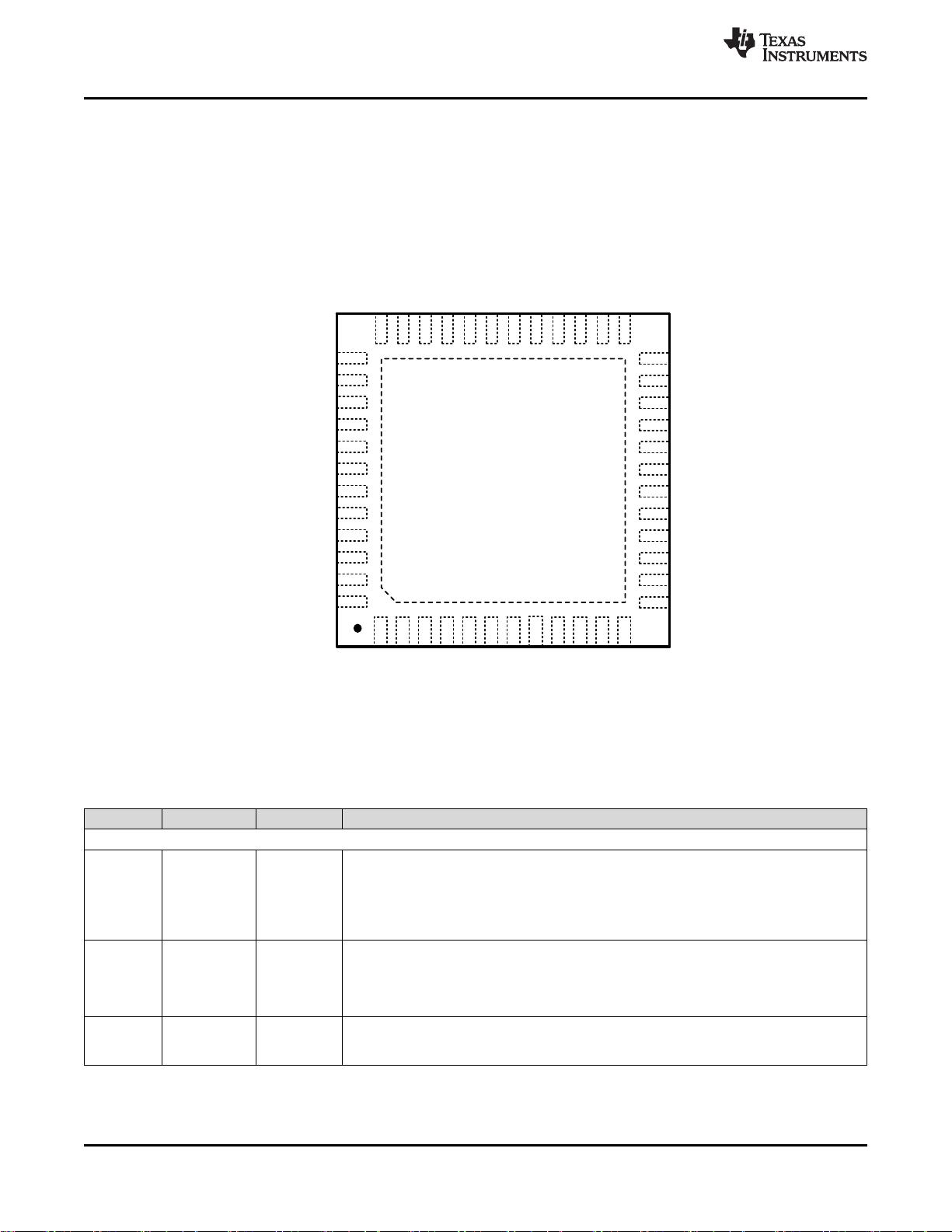
5 Pin Configuration and Functions......................... 4
8.2 Typical Application .................................................. 38
6 Specifications......................................................... 7
9 Power Supply Recommendations...................... 41
6.1 Absolute Maximum Ratings ..................................... 7
9.1 Power Up Requirements and PDB Pin................... 41
6.2 Handling Ratings....................................................... 7
9.2 CML Interconnect Guidelines.................................. 41
6.3 Recommended Operating Conditions....................... 7
10 Layout................................................................... 42
6.4 Thermal Information.................................................. 8
10.1 Layout Guidelines ................................................. 42
6.5 DC Electrical Characteristics .................................... 8
10.2 Layout Example .................................................... 43
6.6 AC Electrical Characteristics................................... 10
11 器器件件和和文文档档支支持持 ..................................................... 45
6.7 Recommended Timing for the Serial Control Bus .. 11
11.1 文档支持................................................................ 45
6.8 Switching Characteristics........................................ 13
11.2 商标 ....................................................................... 45
6.9 Typical Charateristics ............................................. 14
11.3 静电放电警告......................................................... 45
7 Detailed Description............................................ 15
11.4 术语表 ................................................................... 45
7.1 Overview ................................................................. 15
12 机机械械封封装装和和可可订订购购信信息息 .......................................... 45
7.2 Functional Block Diagram ....................................... 15
7.3 Feature Description................................................. 15
4 修修订订历历史史记记录录
NOTE: Page numbers for previous revisions may differ from page numbers in the current version.
Changes from Revision C (April 2013) to Revision D Page
• 已添加 数据表流程和版面布局,以符合全新 TI 标准。 已添加以下章节:处理额定值、器件功能模式;编程;电源建
议;布局布线;器件和文档支持;机械封装和订购信息 ......................................................................................................... 1
• 已添加 器件信息表 .................................................................................................................................................................. 1
• Fixed typo for GPIO configuration ........................................................................................................................................ 19
• Removed two MODE_SEL modes: I2S Channel B, and Backward Compatible.................................................................. 23
• Removed IDx addresses 0x22, 0x24, 0x2E, 0x30, 0x32, 0x34............................................................................................ 26
• Changed suggested resistor values for IDx addresses 0x1E, 0x20, 0x26, 0x28, 0x2A....................................................... 26
Changes from Revision B (August 2012) to Revision C Page
• 已更改 国家数据表布局至 TI 格式。 ....................................................................................................................................... 1
Changes from Revision A (July 2012) to Revision B Page
• Added typical charateristic graphics..................................................................................................................................... 14
• Added” Note: frequency range = 15 - 65MHz when LFMODE = 0 and frequency range = 5 - <15MHz when
LFMODE = 1.” under Functional Description. ...................................................................................................................... 16
• Reformatted Table 2 and added clarification to notes.......................................................................................................... 19
• Added clarification to notes on Table 6, address 0x04[3:0] (backwards compatible and LFMODE registers). .................. 27
Changes from Original (March 2012) to Revision A Page
• 已转换为混合 TI 格式。 .......................................................................................................................................................... 1
• Corrected typo in SCL from pin 6 to pin 8.............................................................................................................................. 4
• Corrected typo in SDA from pin 7 to pin 9.............................................................................................................................. 4
2 Copyright © 2012–2014, Texas Instruments Incorporated

DS90UB925Q-Q1
www.ti.com.cn
ZHCSCX8D –APRIL 2012–REVISED OCTOBER 2014
• Added to Absolute Maximum Rating section, note (3): The maximum limit (V
DDIO
+0.3V) does not apply to the PDB
pin during the transition to the power down state (PDB transitioning from HIGH to LOW).................................................... 7
• Deleted derate from Maximum Power Dissipation Capacity at 25° C. .................................................................................... 7
• Added "Note: BIST is not available in backwards compatible mode." ................................................................................. 20
• Corrected typo in Table 4 "I2S Channel B (18-bit Mode)" from L to H ............................................................................... 23
• Corrected typo in Table 5 Ideal V
R2
(V) from 2.475 to 1.475. .............................................................................................. 26
Copyright © 2012–2014, Texas Instruments Incorporated 3

DIN2 / R2
DIN9 / G1 / GPIO3
DS90UB925Q-Q1
TOP VIEW
B6 / DIN22
B7 / DIN23
HS
VS
DE
CAPL12
SCL
SDA
PCLK
GPO_REG6 / I2S_DA
GPO_REG7 / I2S_WC
I2S_CLK / GPO_REG8
CAPP12
RES0
NC
CAPHS12
RES1
DOUT-
DOUT+
PDB
VDD33
CMF
MODE_SEL
DIN1 / R1 / GPIO1
DIN3 / R3
DIN4 / R4
VDDIO
INTB
DIN5 / R5
DIN6 / R6
DIN7 / R7
B5 / DIN21
B4 / DIN20
B3 / DIN19
B2 / DIN18
I2S_DB / GPO_REG5 / B1 / DIN17
GPO_REG4 / B0 / DIN16
G7 / DIN15
G6 / DIN14
G5 / DIN13
G4 / DIN12
G3 / DIN11
G2 / DIN10
DAP = GND
IDx
13
14
15
16
17
18
19
20
21
22
23
24
1
2
3
4
5
7
8
9
10
11
12
6
48
47
46
45
42
41
40
39
38
37
25
27
36
35
26
28
29
30
31
32
33
34
44
43
DIN8 / G0 / GPIO2
DIN0 / R0 / GPIO0
DS90UB925Q-Q1
ZHCSCX8D –APRIL 2012–REVISED OCTOBER 2014
www.ti.com.cn
5 Pin Configuration and Functions
DS90UB925Q-Q1
48 Pin WQFN
Top View
Pin Functions
PIN NAME PIN # I/O, TYPE DESCRIPTION
LVCMOS PARALLEL INTERFACE
DIN[23:0] / 25, 26, 27, 28, I, LVCMOS Parallel Interface Data Input Pins
R[7:0], 29, 32, 33, 34, w/ pull down Leave open if unused
G[7:0], 35, 36, 37, 38, DIN0 / R0 can optionally be used as GPIO0 and DIN1 / R1 can optionally be used as GPIO1
B[7:0] 39, 40, 41, 42, DIN8 / G0 can optionally be used as GPIO2 and DIN9 /G1 can optionally be used as GPIO3
43, 44, 45, 46, DIN16 / B0 can optionally be used as GPIO4 and DIN17 / B1 can optionally be used as
47, 48, 1, 2 GPIO5
HS 3 I, LVCMOS Horizontal Sync Input Pin
w/ pull down Video control signal pulse width must be 3 PCLKs or longer to be transmitted when the
Control Signal Filter is enabled. There is no restriction on the minimum transition pulse when
the Control Signal Filter is disabled. The signal is limited to 2 transitions per 130 PCLKs.
See Table 6.
VS 4 I, LVCMOS Vertical Sync Input Pin
w/ pull down Video control signal is limited to 1 transition per 130 PCLKs. Thus, the minimum pulse width
is 130 PCLKs.
4 Copyright © 2012–2014, Texas Instruments Incorporated

DS90UB925Q-Q1
www.ti.com.cn
ZHCSCX8D –APRIL 2012–REVISED OCTOBER 2014
Pin Functions (continued)
PIN NAME PIN # I/O, TYPE DESCRIPTION
DE 5 I, LVCMOS Data Enable Input Pin
w/ pull down Video control signal pulse width must be 3 PCLKs or longer to be transmitted when the
Control Signal Filter is enabled. There is no restriction on the minimum transition pulse when
the Control Signal Filter is disabled. The signal is limited to 2 transitions per 130 PCLKs.
See Table 6.
PCLK 10 I, LVCMOS Pixel Clock Input Pin. Strobe edge set by RFB configuration register. See Table 6.
w/ pull down
I2S_CLK, 13, 12, 11 I, LVCMOS Digital Audio Interface Data Input Pins
I2S_WC, w/ pull down Leave open if unused
I2S_DA I2S_CLK can optionally be used as GPO_REG8, I2S_WC can optionally be used as
GPO_REG7, and I2S_DA can optionally be used as GPO_REG6.
OPTIONAL PARALLEL INTERFACE
I2S_DB 44 I, LVCMOS Second Channel Digital Audio Interface Data Input pin at 18–bit color mode and set by
w/ pull down MODE_SEL pin or configuration register
Leave open if unused
I2S_DB can optionally be used as DIN17 or GPO_REG5.
GPIO[3:0] 36, 35, 26, 25 I/O, LVCMOS General Purpose IOs. Available only in 18-bit color mode, and set by MODE_SEL pin or
w/ pull down configuration register. See Table 6.
Leave open if unused.
Shared with DIN9, DIN8, DIN1 and DIN0
GPO_REG[ 13, 12, 11, 44, O, LVCMOS General Purpose Outputs and set by configuration register. See Table 6.
8:4] 43 w/ pull down Share with I2S_CLK, I2S_WC, I2S_DA, I2S_DB or DIN17, DIN16.
CONTROL
PDB 21 I, LVCMOS Power-down Mode Input Pin
w/ pull-down PDB = H, device is enabled (normal operation)
Refer to Power Up Requirements and PDB Pin section.
PDB = L, device is powered down.
When the device is in the powered down state, the Driver Outputs are both HIGH, the PLL is
shutdown, and IDD is minimized. Control Registers are RESET.
MODE_SEL 24 I, Analog Device Configuration Select. See Table 4.
I
2
C
IDx 6 I, Analog I
2
C Serial Control Bus Device ID Address Select
External pull-up to V
DD33
is required under all conditions, DO NOT FLOAT.
Connect to external pull-up and pull-down resistor to create a voltage divider. See Figure 19.
SCL 8 I/O, LVCMOS I
2
C Clock Input / Output Interface
Open Drain Must have an external pull-up to V
DD33
, DO NOT FLOAT.
Recommended pull-up: 4.7kΩ.
SDA 9 I/O, LVCMOS I
2
C Data Input / Output Interface
Open Drain Must have an external pull-up to V
DD33
, DO NOT FLOAT.
Recommended pull-up: 4.7kΩ.
STATUS
INTB 31 O, LVCMOS Interrupt
Open Drain INTB = H, normal
INTB = L, Interrupt request
Recommended pull-up: 4.7kΩ to V
DDIO
FPD-LINK III SERIAL INTERFACE
DOUT+ 20 O, LVDS True Output
The output must be AC-coupled with a 0.1µF capacitor.
DOUT- 19 O, LVDS Inverting Output
The output must be AC-coupled with a 0.1µF capacitor.
CMF 23 Analog Common Mode Filter.
Connect 0.1µF to GND
Copyright © 2012–2014, Texas Instruments Incorporated 5
剩余50页未读,继续阅读
资源评论


不觉明了
- 粉丝: 834
- 资源: 4209
上传资源 快速赚钱
我的内容管理 收起
我的资源 快来上传第一个资源
我的收益
登录查看自己的收益我的积分 登录查看自己的积分
我的C币 登录后查看C币余额
我的收藏
我的下载
下载帮助


会员权益专享
安全验证
文档复制为VIP权益,开通VIP直接复制
