没有合适的资源?快使用搜索试试~ 我知道了~
TI-DS90UB662-Q1.pdf
需积分: 10 0 下载量 82 浏览量
2023-02-01
23:09:58
上传
评论 4
收藏 4.38MB PDF 举报
温馨提示
试读
169页
FPD-Link解串器
资源推荐
资源详情
资源评论
DS90UB662-Q1 Quad 3-Gbps FPD-Link III Deserializer Hub With Single CSI-2 Output
Port
1 Features
• AEC-Q100 qualified for automotive applications:
– Device temperature grade 2: –40℃ to +105℃
ambient operating temperature range
– Device HBM ESD classification Level ±3 kV
– Device CDM ESD classification Level C5
• Quad deserializer hub aggregates data from up to
4 sensors simultaneously supports
• Supports 1-Megapixel sensors up to 60-Hz frame
rate and 2-Megapixel sensors up to 30-Hz frame
rate
• Precise multi-camera synchronization
• MIPI DPHY version 1.2 / CSI-2 version 1.3
compliant
– 1 × CSI-2 MIPI Output Port
– Supports 1, 2, 3, 4 data lanes
– CSI-2 data rate scalable for 400 Mbps / 800
Mbps / 1.2 Gbps / 1.5 Gbps / 1.6 Gbps per lane
• Ultra-low data and control path latency
• Supports single-ended coaxial including Power-
over-Coax (PoC) or Shielded Twisted-Pair (STP)
cable
• Adaptive receive equalization
• Dual I2C ports with fast-mode plus up to 1 Mbps
• Flexible GPIOs for sensor synchronization and
diagnostics
• Compatible with DS90UB633A-Q1 serializer and
DS90UB63x CSI-2 Serializers
• Internal programmable precision frame sync
generator
• Line fault detection and advanced diagnostics
• Functional Safety-Capable
– Documentation available to aid ISO 26262
system design
2 Applications
• Automotive ADAS
– Rear View Cameras (RVC)
– Surround View Systems (SVS)
– Camera Monitoring Systems (CMS)
– Forward Vision Cameras (FC)
– Driver Monitoring Systems (DMS)
– Satellite RADAR, Time-of-Flight (ToF), and
LIDAR sensors modules
– Sensor fusion
• Security and Surveillance
3 Description
The DS90UB662-Q1 is a versatile sensor hub
capable of connecting serialized sensor data received
from four independent video data streams through a
FPD-Link III interface. When paired with a
DS90UB633A-Q1 or DS90UB63x CSI-2 serializer, the
DS90UB662-Q1 receives data from 1-Megapixel
image sensors supporting 720p/800p/960p/1MP
resolution at 30-Hz or 60-Hz frame rates. Data is
received and aggregated into a MIPI CSI-2 compliant
output for interconnect to a downstream processor.
The DS90UB662-Q1 includes four FPD-Link III
deserializers, each enabling a connection through
cost-effective 50-Ω single-ended coaxial or 100-Ω
differential STP cables. The receive equalizers
automatically adapt to compensate for cable loss
characteristics, including degradation over time.
Each of the FPD-Link III interfaces also includes a
separate low latency bidirectional control channel that
continuously conveys I2C, GPIOs, and other control
information. General-purpose I/O signals such as
those required for camera synchronization and
diagnostics features also make use of this
bidirectional control channel.
The DS90UB662-Q1 is AEC-Q100 qualified for
automotive applications and is offered in a cost-
effective and space-saving 64-pin VQFN package.
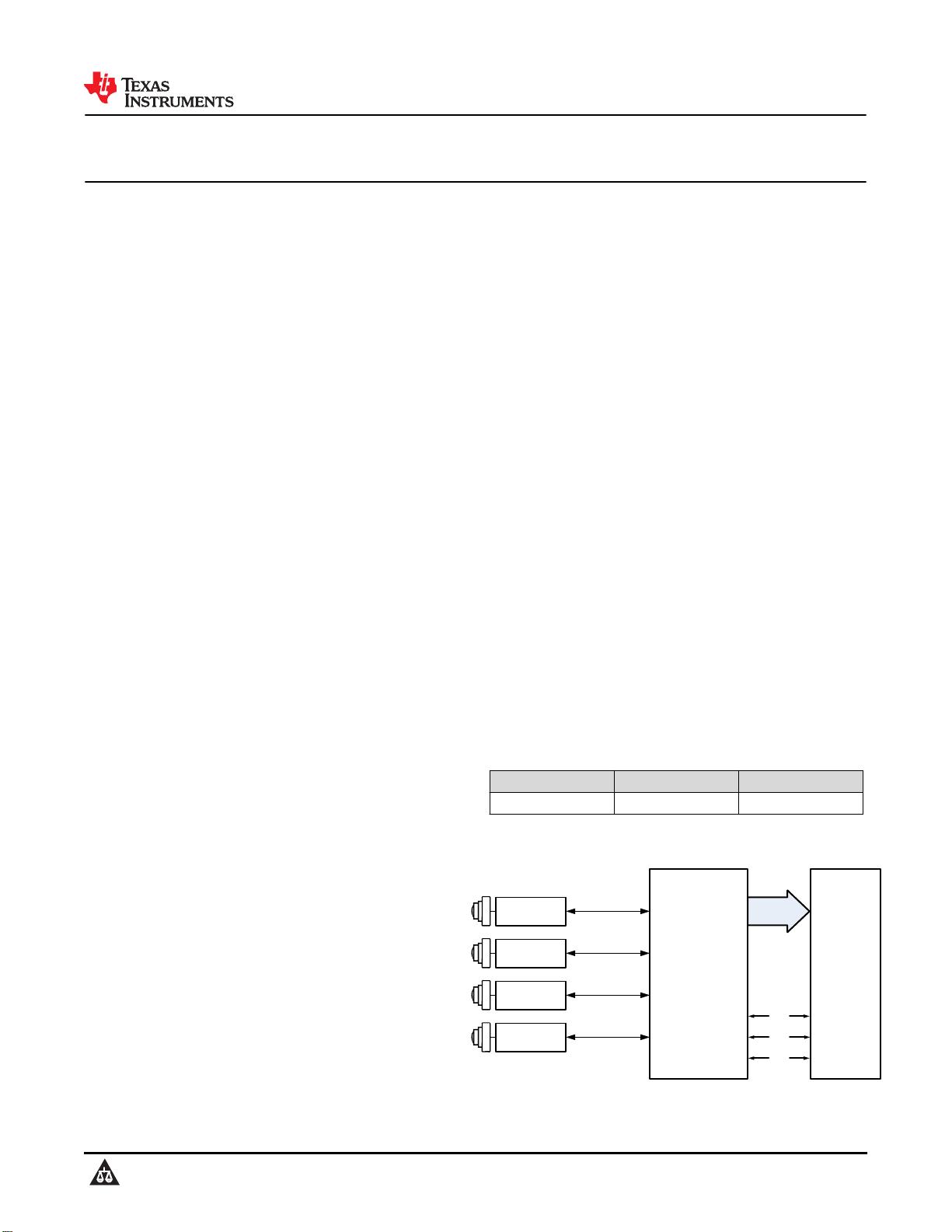
Device Information
PART NUMBER
(1)
PACKAGE BODY SIZE (NOM)
DS90UB662-Q1 VQFN (64) 9.00 mm × 9.00 mm
(1) For all available packages, see the orderable addendum at
the end of the data sheet.
MIPI CSI-2
Processor
SoC
DS90UB662-Q1
FPD-Link III HUB
FPD-Link III
Serializer
I2C
FPD-Link III
Coax or STP
FPD-Link III
Serializer
FPD-Link III
Serializer
FPD-Link III
Serializer
TX Port0:
Up to 4 Lanes
GPIO
INTB
Typical Application Schematic
www.ti.com
DS90UB662-Q1
SNLS675A – NOVEMBER 2020 – REVISED NOVEMBER 2020
Copyright © 2020 Texas Instruments Incorporated
Submit Document Feedback
1
DS90UB662-Q1
SNLS675A – NOVEMBER 2020 – REVISED NOVEMBER 2020
An IMPORTANT NOTICE at the end of this data sheet addresses availability, warranty, changes, use in safety-critical applications,
intellectual property matters and other important disclaimers. PRODUCTION DATA.
Table of Contents
1 Features............................................................................1
2 Applications..................................................................... 1
3 Description.......................................................................1
4 Revision History.............................................................. 2
5 Pin Configuration and Functions...................................3
Pin Functions.................................................................... 4
6 Specifications.................................................................. 7
6.1 Absolute Maximum Ratings........................................ 7
6.2 ESD Ratings............................................................... 7
6.3 Recommended Operating Conditions.........................7
6.4 Thermal Information....................................................8
6.5 DC Electrical Characteristics...................................... 8
6.6 AC Electrical Characteristics.....................................12
6.7 CSI-2 Timing Specifications...................................... 13
6.8 Recommended Timing for the Serial Control Bus.....17
6.9 Typical Characteristics.............................................. 22
7 Detailed Description......................................................23
7.1 Overview................................................................... 23
7.2 Functional Block Diagram......................................... 24
7.3 Feature Description...................................................24
7.4 Device Functional Modes..........................................24
7.5 Programming............................................................ 52
7.6 Register Maps...........................................................67
8 Application and Implementation................................ 139
8.1 Application Information........................................... 139
8.2 Typical Application.................................................. 143
8.3 System Example..................................................... 146
9 Power Supply Recommendations..............................148
9.1 VDD Power Supply................................................. 148
9.2 Power-Up Sequencing............................................ 148
10 Layout.........................................................................151
10.1 Layout Guidelines................................................. 151
10.2 Layout Example.................................................... 153
11 Device and Documentation Support........................157
11.1 Documentation Support........................................ 157
11.2 Receiving Notification of Documentation Updates 157
11.3 Support Resources............................................... 157
11.4 Trademarks........................................................... 157
11.5 Electrostatic Discharge Caution............................ 157
11.6 Glossary................................................................ 157
12 Mechanical, Packaging, and Orderable
Information.................................................................. 157
12.1 Package Option Addendum.................................. 158
4 Revision History
NOTE: Page numbers for previous revisions may differ from page numbers in the current version.
Changes from Revision * (December 2016) to Revision A (September 2018) Page
• Updated marketing status from Advance Information to production data. .........................................................1
DS90UB662-Q1
SNLS675A – NOVEMBER 2020 – REVISED NOVEMBER 2020
www.ti.com
2 Submit Document Feedback
Copyright © 2020 Texas Instruments Incorporated
5 Pin Configuration and Functions
RIN0-
PDB
RES
VDD18_P2
VDD18_FPD1
CMLOUTN
CMLOUTP
VDD18_FPD2
RIN2+
RIN2-
GPIO3
CSI0_D2P
CSI0_CLKP
VDD18_P0
CSI
0_D3N
CSI0_D3P
GPIO0
I2C_SCL2
CSI0_D1P
CSI0_D2N
VDDIO
CSI0_D1N
VDD_CSI0
CSI0_CLKN
RIN3+
VDD_FPD2
VDD18_P3
RIN3-
VDD18_FPD3
1
2
3
4
5
6
7
8
9
10
11
12
13
14
15
16
32
31
30
29
28
27
26
25
24
23
22
21
20
19
18
17
48
47
46
45
44
43
42
41
40
39
38
37
36
35
34
33
49
50
51
52
53
54
55
56
57
58
59
60
61
62
63
64
VDD_FPD1
NC
NC
RIN1-
GPIO7
GPIO5
GPIO6
NC
VDD18_FPD0
RIN0+
NC
NC
NC
INTB
I2C_SDA2
CSI0_D0P
CSI0_D0N
VDDL2
VDD18_P1
MODE
IDX
GPIO2
VDDL1
I2C_SCL
I2C_SDA
VDD_CSI1
NC
NC
NC
GPIO1
VDD18A
RIN1+
NC
REFCLK
DS90UB662-Q1
64L QFN
Top down view
DAP
GPIO4
Figure 5-1. RTD Package 64-Pin VQFN (Top View)
www.ti.com
DS90UB662-Q1
SNLS675A – NOVEMBER 2020 – REVISED NOVEMBER 2020
Copyright © 2020 Texas Instruments Incorporated
Submit Document Feedback
3
Pin Functions
PIN I/O
TYPE
DESCRIPTION
NAME NO.
MIPI CSI-2 TX INTERFACE
CSI_CLKN 22 O CSI-2 differential clock output pins.
Leave unused pins as No Connect.
CSI_CLKP 23
CSI_D0N 24 CSI-2 differential data output pins. Use CSI_PORT_SEL (see Table 7-68), CSI_CTL
(see Table 7-69), and CSI_CTL2 (see Table 7-70) registers for the CSI-2 TX control.
Leave unused pins as No Connect.
CSI_D0P 25
CSI_D1N 26
CSI_D1P 27
CSI_D2N 28
CSI_D2P 29
CSI_D3N 30
CSI_D3P 31
FPD-LINK III RX INTERFACE
RIN0+ 50 I/O FPD-Link III RX Port 0 pins. The port receives FPD-Link III high-speed forward
channel video and control data and transmits back channel control data. It can
interface with a compatible FPD-Link III serializer TX through a STP or coaxial cable
(see Figure 8-6 and Figure 8-7). It must be AC-coupled per Table 8-4.
If port is unused, set RX_PORT_CTL register bit 0 to 0 to disable RX Port 0 (see Table
7-30) and leave the pins as No Connect.
RIN0- 51
RIN1+ 53 FPD-Link III RX Port 1 pins. The port receives FPD-Link III high-speed forward
channel video and control data and transmits back channel control data. It can
interface with a compatible FPD-Link III serializer TX through a STP or coaxial cable
(see Figure 8-6 and Figure 8-7). It must be AC-coupled per Table 8-4.
If port is unused, set RX_PORT_CTL register bit 1 to 0 to disable RX Port 1 (see Table
7-30) and leave the pins as No Connect.
RIN1- 54
RIN2+ 59 FPD-Link III RX Port 2 pins. The port receives FPD-Link III high-speed forward
channel video and control data and transmits back channel control data. It can
interface with a compatible FPD-Link III serializer TX through a STP or coaxial cable
(see Figure 8-6 and Figure 8-7). It must be AC-coupled per Table 8-4.
If port is unused, set RX_PORT_CTL register bit 2 to 0 to disable RX Port 2 (See Table
7-30) and leave the pins as No Connect.
RIN2- 60
RIN3+ 62 FPD-Link III RX Port 3 pins. The port receives FPD-Link III high-speed forward
channel video and control data and transmits back channel control data. It can
interface with a compatible FPD-Link III serializer TX through a STP or coaxial cable
(see Figure 8-6 and Figure 8-7). It must be AC-coupled per Table 8-4.
If port is unused, set RX_PORT_CTL register bit 3 to 0 to disable RX Port 3 (see Table
7-30) and leave the pins as No Connect.
RIN3- 63
SYNCHRONIZATION AND GENERAL-PURPOSE I/O
GPIO0 9 I/O, PD General-Purpose Input/Output pins. The pins can be used to control and respond to
various commands. They may be configured to be input signals for the corresponding
GPIOs on the serializer or they may be configured to be outputs to follow local register
settings. At power up, the GPIO pins are disabled and by default include a pulldown
resistor (25-kΩ typ).
See Section 7.4.11. for programmability. If unused, leave the pin as No Connect.
GPIO1 10
GPIO2 14
GPIO3 15
GPIO4 17
GPIO5 18
GPIO6 19
GPIO7 20
INTB 6 O, OD Interrupt Output pin.
INTB is an active-low open drain and controlled by the status registers. See Section
7.5.9.
Recommend a 4.7-kΩ Pullup to to 1.8 V or 3.3 V. If unused, leave the pin as No
Connect.
SERIAL CONTROL BUS (I2C)
DS90UB662-Q1
SNLS675A – NOVEMBER 2020 – REVISED NOVEMBER 2020
www.ti.com
4 Submit Document Feedback
Copyright © 2020 Texas Instruments Incorporated
PIN I/O
TYPE
DESCRIPTION
NAME NO.
I2C_SCL 12 I/O, OD Primary I2C Clock Input / Output interface pin. See Section 7.5.1.
Recommend a 2.2-kΩ to 4.7-kΩ Pullup
(1)
to 1.8 V or 3.3 V.
I2C_SDA 11 I/O, OD Primary I2C Data Input / Output interface pin. See Section 7.5.1.
Recommend a 2.2-kΩ to 4.7-kΩ Pullup
(1)
to 1.8 V or 3.3 V.
I2C_SCL2 8 I/O, OD Secondary I2C Clock Input / Output interface pin. See Section 7.5.2.
Recommend a 2.2-kΩ to 4.7-kΩ Pullup
(1)
to 1.8 V or 3.3 V.
I2C_SDA2 7 I/O, OD Secondary I2C Data Input / Output interface pin. See Section 7.5.2.
Recommend a 2.2-kΩ to 4.7-kΩ Pullup
(1)
to 1.8 V or 3.3 V.
CONFIGURATION AND CONTROL
IDX 46 S I2C Serial Control Bus Device ID Address Select configuration pin.
Connect to an external pullup to VDD18 and a pulldown to GND to create a voltage
divider. See Table 7-15.
MODE 45 S Mode Select configuration pin.
Connect to external pullup to VDD18 and a pulldown to GND to create a voltage
divider. See Table 7-1.
PDB 3 I, PD Inverted Power-Down input pin. Typically connected to a processor GPIO with a
pulldown. When PDB input is brought HIGH, the device is enabled and internal
registers and state machines are reset to default values. Asserting PDB signal low will
power down the device and consume minimum power. The default function of this pin
is PDB = LOW; POWER DOWN with an internal 50-kΩ internal pulldown enabled.
PDB should remain low until after power supplies are applied and reach minimum
required levels. See Section 9.1.
INPUT IS 3.3-V TOLERANT
PDB = 1.8 V, device is enabled (normal operation)
PDB = 0 V, device is powered down.
POWER AND GROUND
VDDIO 16 P 1.8-V (±5%) OR 3.3-V (±10%) LVCMOS I/O Power
Requires 1-μF and 0.1-μF or 0.01-μF capacitors to GND.
VDD_CSI
VDD_CSI
21
33
P 1.1-V (±5%) Power Supplies
Requires 0.1-μF or 0.01-μF capacitors to GND at each VDD pin. Additional 1-μF and
10-μF decoupling is recommended for the pin group.
VDDL1
VDDL2
13
44
P 1.1-V (±5%) Power Supplies
Requires 0.1-μF or 0.01-μF capacitors to GND at each VDD pin. Additional 1-μF and
10-μF decoupling is recommended for the pin group.
VDD_FPD1
VDD_FPD2
52
61
P 1.1-V (±5%) Power Supplies
Requires 0.1-μF or 0.01-μF capacitors to GND at each VDD pin. Additional 1-μF and
10-μF decoupling is recommended for the pin group.
VDD18_P2
VDD18_P3
VDD18_P1
VDD18_P0
2
1
47
48
P
1.8-V (±5%) Power Supplies
Requires 0.1-μF or 0.01-μF capacitors to GND at each VDD pin. Additional 1-μF, and
10-μF decoupling is recommended for the pin group.
VDD18A 32 P 1.8-V (±5%) Power Supplies
Requires 0.1-μF or 0.01-μF capacitors to GND at each VDD pin. Additional 1-μF, and
10-μF decoupling is recommended for the pin group.
VDD18_FPD0
VDD18_FPD1
VDD18_FPD2
VDD18_FPD3
49
55
58
64
P
1.8-V (±5%) Power Supplies
Requires 0.1-μF or 0.01-μF capacitors to GND at each VDD pin. Additional 1-μF, and
10-μF decoupling is recommended for the pin group.
GND DAP G DAP is the large metal contact at the bottom side, located at the center of the VQFN
package. Connect to the ground plane (GND).
OTHERS
REFCLK 5 I Reference clock oscillator input.
Typically connected to a 23-MHz to 26-MHz LVCMOS-level oscillator (100 ppm).
For 400-Mbps, 800-Mbps or 1.6-Gbps CSI-2 data rates, use 25-MHz frequency.
For the oscillator requirements, see Section 7.4.4. For other common CSI-2 data rates,
see Section 7.4.19.
RES 4 - This pin must be tied to GND for normal operation.
www.ti.com
DS90UB662-Q1
SNLS675A – NOVEMBER 2020 – REVISED NOVEMBER 2020
Copyright © 2020 Texas Instruments Incorporated
Submit Document Feedback
5
剩余168页未读,继续阅读
资源评论
不觉明了
- 粉丝: 3132
- 资源: 5370
上传资源 快速赚钱
- 我的内容管理 展开
- 我的资源 快来上传第一个资源
- 我的收益 登录查看自己的收益
- 我的积分 登录查看自己的积分
- 我的C币 登录后查看C币余额
- 我的收藏
- 我的下载
- 下载帮助
安全验证
文档复制为VIP权益,开通VIP直接复制
信息提交成功