TI-DS90UB949A-Q1.pdf
需积分: 9 117 浏览量
2023-02-01
22:52:27
上传
评论 4
收藏 2.1MB PDF 举报

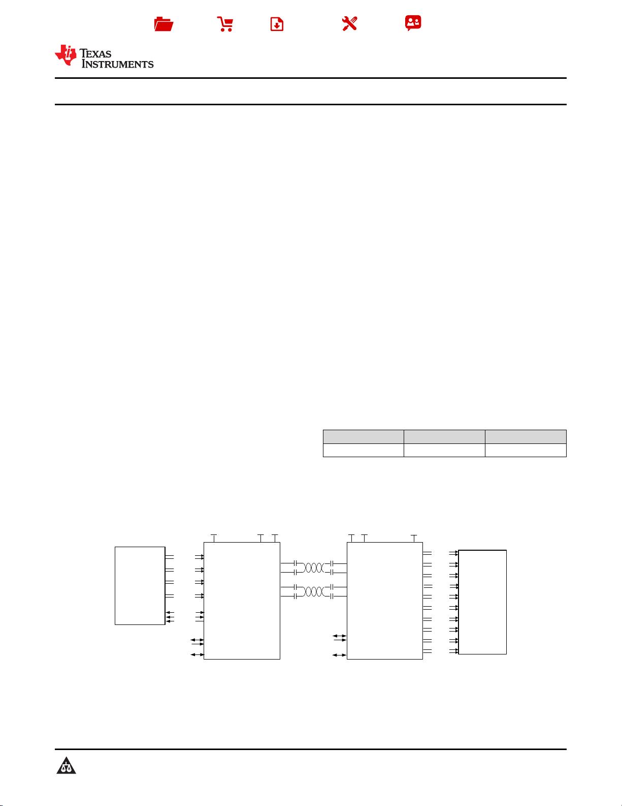
FPD-Link III
2 Lane
VDDIO
1.8 V
IDx
DOUT0+
DOUT0-
1.1V
IN_CLK-/+
HDMI
HPD
DDC
CEC
DOUT1+
DOUT1-
RIN0+
RIN0-
RIN1+
RIN1-
CLK1+/-
CLK2+/-
oLDI
D0+/-
D1+/-
D2+/-
D3+/-
D4+/-
D5+/-
D6+/-
D7+/-
DS90UB949A-Q1
Serializer
DS90UB948-Q1
Deserializer
IDx
D_GPIO
(SPI)
D_GPIO
(SPI)
LVDS Display
(2880x1080)
or Graphic
Processor
Graphics
Processor
IN_D0-/+
IN_D1-/+
IN_D2-/+
I2C
VDDIO
(3.3 V / 1.8 V)
3.3 V
I2C
1.25 V
1.8V
HDMI ± High Definition Multimedia Interface
Product
Folder
Order
Now
Technical
Documents
Tools &
Software
Support &
Community
本文档旨在为方便起见,提供有关 TI 产品中文版本的信息,以确认产品的概要。 有关适用的官方英文版本的最新信息,请访问 www.ti.com,其内容始终优先。 TI 不保证翻译的准确
性和有效性。 在实际设计之前,请务必参考最新版本的英文版本。
English Data Sheet: SNLS650
DS90UB949A-Q1
ZHCSJR7 –MAY 2019
DS90UB949A-Q1 2K HDMI 转转 FPD-Link III 桥桥接接器器串串行行器器
1
1 特特性性
1
• 符合面向汽车应用的 AEC-Q100 标准AEC-Q100
标准:
– 器件温度等级 2:–40°C 至 105°C,T
A
• 支持高达 210MHz 的 TMDS 时钟频率,可实现 3K
(2880x1620)(30Hz 频率)、QXGA
(2048x1536)、2K (2880x1080)、WUXGA
(1920x1200) 或 1080p60(24 位色深)
• 单路和双路 FPD-Link III 输出,支持 STP 或 STQ
或同轴电缆
• 高清多媒体 (HDMI) v1.4b 兼容输入
• HDMI 模式 DisplayPort (DP++) 输入
• 最多支持 8 通道的 HDMI 音频提取
• 高速反向通道,支持高达 2Mbps 的 GPIO
• 可跟踪扩频输入时钟以降低 EMI
• 具有 1Mbps 快速模式增强版的 I2C(主/从)
• SPI 直通接口
• 向后兼容 DS90UB926Q-Q1、DS90UB928Q-Q1
和 DS90UB924-Q1 FPD-Link III 解串器
2 应应用用
• 汽车信息娱乐系统和仪表组
– 汽车音响主机
– 汽车后座娱乐显示屏
– 汽车中心信息显示屏
– 商用车辆仪表组
– 汽车媒体中心
• 音频/视频控制系统
3 说说明明
DS90UB949A-Q1 是一款 HDMI 转 FPD-Link III 桥接
器件,当与 FPD-Link III DS90UB940-
Q1/DS90UB948-Q1 解串器配合使用时,可通过具有
成本效益的 50Ω 单端同轴电缆或 100Ω 差分屏蔽双绞
线 (STP) 和屏蔽四路绞线 (STQ) 电缆提供单通道或双
通道高速串行流。该器件可对 HDMI v1.4b 输入进行序
列化,从而支持在 60Hz 下实现高达 2880x1080 且具
有 24 位色深的视频分辨率。
FPD-Link III 接口支持通过同一条差分链路进行视频和
音频数据传输以及全双工控制(包括 I2C 和 SPI 通
信)。通过两个差分对进行视频数据整合和控制,有助
于减小应用的互连线尺寸和重量,并简化系统设计。通
过使用低压差分信令、数据换序和随机生成最大限度减
少了 EMI。在向后兼容模式中,当 DS90UB949A-Q1
与 DS90Ux92x-Q1 解串器配合使用时,可通过在单一
差分链路支持高达 1920x720 且具有 24 位色深的分辨
率。
DS90UB949A-Q1 支持通过 外部 I2S 接口接收多通道
音频。该器件还具有可选的辅助音频接口。
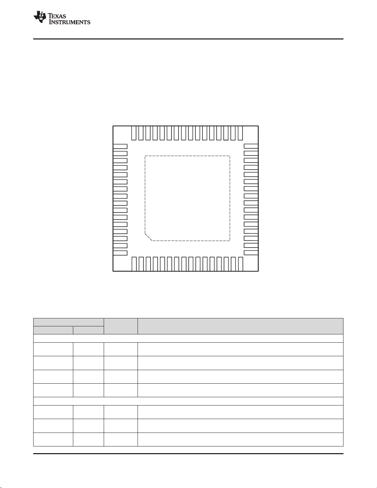
器器件件信信息息
(1)
器器件件型型号号 封封装装 封封装装尺尺寸寸((标标称称值值))
DS90UB949A-Q1 VQFN (64) 9.00mm x 9.00mm
(1) 如需了解所有可用封装,请参阅数据表末尾的可订购产品附
录。
应应用用 图图
剩余83页未读,继续阅读
资源评论


