没有合适的资源?快使用搜索试试~ 我知道了~
TI-TPD3S713-Q1.pdf
需积分: 9 0 下载量 99 浏览量
2022-11-16
21:19:29
上传
评论 5
收藏 4.04MB PDF 举报
温馨提示
试读
38页
TI-TPD3S713-Q1.pdf
资源推荐
资源详情
资源评论
Product
Folder
Order
Now
Technical
Documents
Tools &
Software
Support &
Community
Reference
Design
An IMPORTANT NOTICE at the end of this data sheet addresses availability, warranty, changes, use in safety-critical applications,
intellectual property matters and other important disclaimers. PRODUCTION DATA.
TPD3S713-Q1
SLUSDH1 –MAY 2020
TPD3S713-Q1 Automotive USB 2.0 Interface Protection with Adjustable Current Limit and
Short-to-V
BATT
Protection
1
1 Features
1
• AEC-Q100 Qualified for automotive applications:
– Device temperature grade 1: –40°C to +125°C
ambient operating temperature range
– Device HBM ESD classification level H2
– Device CDM ESD classification level C5
• Short-to-Battery (up to 18 V) and Short-to-Ground
protection on V
BUS
pin
• Short-to-Battery (up to 18 V) and Short-to-V
BUS
protection on DM_IN, DP_IN pins
• DP_IN and DM_IN IEC 61000-4-2 Rated
– ±8-kV Contact and ±15-kV air discharge
• High speed data switches (1230 MHz BW)
• 4.5-V to 5.5-V Input operating range
• 50-mA to 600-mA adjustable current limit (±13.5%
at 200 mA)
• Integrated 73-mΩ (typical) High-Side MOSFET
• 500-mA Maximum continuous output current
• V
BUS
Cable compensation
• 20-Pin QFN (3-mm × 4-mm) Package
2 Applications
• Automotive USB interface
– Head unit
– Telematics
– Navigation module
• Automotive USB charging ports
– Media interface
3 Description
The TPD3S713-Q1 is a single-chip solution for short-
to-battery, short-circuit, and ESD protection for high
speed data and power lines in automotive USB hub,
head unit, telematics, and media interface
applications. The integrated data switches provide
best-in-class bandwidth for minimal signal
degradation during USB short-to-battery events. The
high bandwidth of 1.2 GHz allows for a clean USB2.0
high-speed 480 Mbps eye diagram with the long
captive cables that are common in the automotive
USB environment.
The short-to-battery protection isolates the internal
system circuits from any overvoltage conditions at the
V
BUS
, DP_IN, and DM_IN pins. On these pins, the
TPD3S713-Q1 can handle overvoltages up to 18 V
for hot plug and DC events and shut off the internal
switches to the upstream transceiver from harmful
voltage and current spikes.
The V
BUS
pin also provides an adjustable current
limited load switch from 50 mA to 600 mA, which
provides flexibility and also saves system power
budget when the port requires only several tens of
milliampere.
The TPD3S713-Q1 device has a current-sense
output that is able to control an upstream supply,
which allows it to maintain 5 V at the remote USB
port connected after a long USB cables.
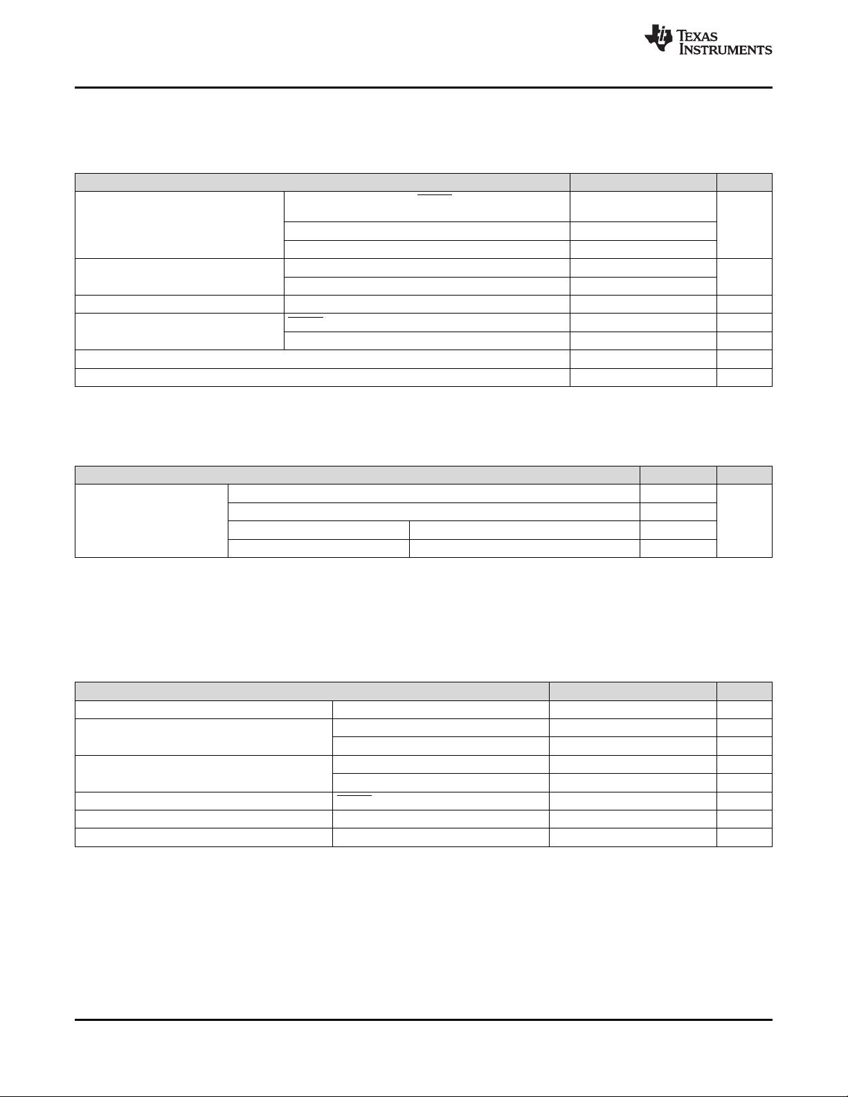
Device Information
(1)
PART NUMBER PACKAGE BODY SIZE (NOM)
TPD3S713-Q1 WQFN (20) 3.00 mm × 4.00 mm
(1) For all available packages, see the orderable addendum at
the end of the data sheet.
Schematic
2
TPD3S713-Q1
SLUSDH1 –MAY 2020
www.ti.com
Product Folder Links: TPD3S713-Q1
Submit Documentation Feedback Copyright © 2020, Texas Instruments Incorporated
Table of Contents
1 Features.................................................................. 1
2 Applications ........................................................... 1
3 Description ............................................................. 1
4 Revision History..................................................... 2
5 Pin Configuration and Functions......................... 3
6 Specifications......................................................... 4
6.1 Absolute Maximum Ratings ...................................... 4
6.2 ESD Ratings.............................................................. 4
6.3 Recommended Operating Conditions....................... 4
6.4 Thermal Information.................................................. 5
6.5 Electrical Characteristics........................................... 5
6.6 Switching Characteristics.......................................... 8
6.7 Typical Characteristics.............................................. 9
7 Parameter Measurement Information ................ 15
8 Detailed Description............................................ 16
8.1 Overview ................................................................. 16
8.2 Functional Block Diagram ....................................... 17
8.3 Feature Description................................................. 17
8.4 Device Functional Modes........................................ 21
9 Application and Implementation ........................ 23
9.1 Application Information............................................ 23
9.2 Typical Application ................................................. 23
10 Power Supply Recommendations ..................... 27
11 Layout................................................................... 27
11.1 Layout Guidelines ................................................. 27
11.2 Layout Example .................................................... 29
12 Device and Documentation Support ................. 30
12.1 Device Support...................................................... 30
12.2 Documentation Support ........................................ 30
12.3 Receiving Notification of Documentation Updates 30
12.4 Support Resources ............................................... 30
12.5 Trademarks........................................................... 30
12.6 Electrostatic Discharge Caution............................ 30
12.7 Glossary................................................................ 30
13 Mechanical, Packaging, and Orderable
Information ........................................................... 30
4 Revision History
DATE REVISION NOTES
May 2020 * Initial Release
Thermal Pad
1
2
3
4
5
6
16
15
14
13
12
11
7 8 9 10
20 19 18 17
EN
IN
DP_OUT
DM_OUT
CS
ILIM_SEL
INT1
IMON
INT2
GND
DP_IN
DM_IN
BUS
NC
FAULT
ILIM_LO
ILIM_HI
IN
BUS
BIAS
3
TPD3S713-Q1
www.ti.com
SLUSDH1 –MAY 2020
Product Folder Links: TPD3S713-Q1
Submit Documentation FeedbackCopyright © 2020, Texas Instruments Incorporated
(1) I = Input, O = Output, I/O = Input and output, PWR = Power
5 Pin Configuration and Functions
RVC Package
20-Pin WQFN
Top View
Pin Functions
PIN
TYPE
(1)
DESCRIPTION
NAME NO.
IMON 1 O
This pin sources a scaled-down ratio of current through the internal FET. A resistor from this pin to
GND converts current to proportional voltage; used as an analog current monitor.
IN 2,3 PWR
Input supply voltage; connect a 0.1-µF or greater ceramic capacitor from IN to GND as close to the
IC as possible.
DM_OUT 4 I/O DM data line to upstream USB host controller
DP_OUT 5 I/O DP data line to upstream USB host controller
CS 6 O Linear cable compensation current. Connect to divider resistor of front-end dc-dc converter.
EN 7 I
Logic-level control input for turning the power and signal switches on or off. When EN is low, the
device is disabled, and the signal and power switches are OFF.
ILIM_SEL 8 I
Logic-level control input for choosing the current limit resistor and current limit threshold. When
ILIM_SEL = High, ILIM_HI resistor is valid; When ILIM_SEL = Low, ILIM_LO resistor is valid.
INT1 9 I
Logic-level control input, the device can be set in normal mode or client mode through pin
configuration. If INT1 = high, the device is in normal mode; If INT1 = low and ILIM_SEL = Low, the
device is in client mode.
INT2 10 I For internal circuit, must connect to ground without a pull down resistor.
GND 11 — Ground connection; should be connected externally to the thermal pad.
BIAS 12 PWR Used for IEC protection. Typically, connect a 2.2-µF capacitor to ground and 5.1 kΩ resistor to BUS.
DP_IN 13 I/O DP data line to downstream connector
DM_IN 14 I/O DM data line to downstream connector
BUS 15,16 PWR Power-switch output
NC 17 NC No connect, leave floating or connect to ground.
FAULT 18 O
Active-low, open-drain output, asserted during overtemperature, overcurrent, and overvoltage
conditions.
ILIM_LO 19 I External resistor used to set the low current-limit threshold, selected by ILIM_SEL pin.
ILIM_HI 20 I External resistor used to set the high current-limit threshold, selected by ILIM_SEL pin.
Thermal pad — Thermal pad on the bottom of the package
4
TPD3S713-Q1
SLUSDH1 –MAY 2020
www.ti.com
Product Folder Links: TPD3S713-Q1
Submit Documentation Feedback Copyright © 2020, Texas Instruments Incorporated
(1) Stresses beyond those listed under Absolute Maximum Ratings may cause permanent damage to the device. These are stress ratings
only, which do not imply functional operation of the device at these or any other conditions beyond those indicated under Recommended
Operating Conditions. Exposure to absolute-maximum-rated conditions for extended periods may affect device reliability.
6 Specifications
6.1 Absolute Maximum Ratings
Voltages are with respect to GND unless otherwise noted
(1)
MIN MAX UNIT
Voltage range
CS, ILIM_SEL, INT1, EN, FAULT, ILIM_HI, ILIM_LO,
IN, IMON, INT2
–0.3 7
V
DM_OUT, DP_OUT –0.3 5.7
BIAS, DM_IN, DP_IN, VBUS –0.3 18
Continuous current
DM_IN to DM_OUT or DP_IN to DP_OUT –100 100
mA
IBUS Internally limited
Continuous output source current, I
SRC
ILIM_HI, LIM_LO, IMON Internally limited A
Continuous output sink current, I
SNK
FAULT 25 mA
CS Internally limited A
Operating junction temperature, T
J
–40 150 °C
Storage temperature,T
stg
–65 150 °C
(1) AEC Q100-002 indicates that HBM stressing shall be in accordance with the ANSI/ESDA/JEDEC JS-001 specification.
(2) The passing level per AEC-Q100 Classification H2.
(3) The passing level per AEC-Q100 Classification C5
(4) Surges per IEC 61000-4-2, level 4, 1999 applied from DP_IN and DM_IN to output ground of the TPD3S713Q1EVM-103 evaluation
module.
6.2 ESD Ratings
VALUE UNIT
V
(ESD)
Electrostatic
discharge
Human-body model (HBM), per AEC Q100-002
(1)
±2000
(2)
V
Charged-device model (CDM), per AEC Q100-011 ±750
(3)
IEC 61000-4-2 contact discharge DP_IN and DM_IN pins
(4)
±8000
IEC 61000-4-2 air discharge DP_IN and DM_IN pins
(4)
±15000
6.3 Recommended Operating Conditions
Voltages are with respect to GND unless otherwise noted.
MIN NOM MAX UNIT
V
(IN)
Supply voltage IN 4.5 5.5 V
Input voltage
EN, ILIM_SEL, INT1, INT2 0 5.5 V
DM_IN, DM_OUT, DP_IN, DP_OUT 0 3.6 V
I
(BUS)
Output continuous current
IBUS 500 mA
DM_IN to DM_OUT or DP_IN to DP_OUT –30 30 mA
Continuous output sink current FAULT 10 mA
R
(ILIM_xx)
Current-limit-set resistors 6.98 100 kΩ
T
J
Operating junction temperature –40 125 °C
5
TPD3S713-Q1
www.ti.com
SLUSDH1 –MAY 2020
Product Folder Links: TPD3S713-Q1
Submit Documentation FeedbackCopyright © 2020, Texas Instruments Incorporated
(1) For more information about traditional and new thermal metrics, see the Semiconductor and IC Package Thermal Metrics application
report.
6.4 Thermal Information
THERMAL METRIC
(1)
TPD3S713-Q1
UNITRVC (WQFN)
20 PINS
R
θJA
Junction-to-ambient thermal resistance 37.9 °C/W
R
θJC(top)
Junction-to-case (top) thermal resistance 39.9 °C/W
R
θJB
Junction-to-board thermal resistance 11.9 °C/W
ψ
JT
Junction-to-top characterization parameter 0.5 °C/W
ψ
JB
Junction-to-board characterization parameter 11.8 °C/W
R
θJC(bot)
Junction-to-case (bottom) thermal resistance 3.2 °C/W
(1) Pulse-testing techniques maintain junction temperature close to ambient temperature. Thermal effects must be taken into account
separately.
(2) This parameter is provided for reference only and does not constitute part of TI's published device specifications for purposes of TI's
product warranty.
6.5 Electrical Characteristics
Unless otherwise noted, –40°C ≤ T
J
≤ 125°C and 4.5 V ≤ V
(IN)
≤ 5.5 V, V
(EN)
= V
(INT1)
= V
(ILIM_SEL)
= V
(IN)
, V
(INT2)
= GND, R
(FAULT)
= 10 kΩ, R
(IMON)
= 2.55 kΩ, R
(ILIM_HI)
= 52.3 kΩ. Positive currents are into pins. Typical values are at T
J
= 25°C. All voltages
are with respect to GND.
PARAMETER TEST CONDITIONS MIN TYP MAX UNIT
OUT – POWER SWITCH
r
DS(on)
On-resistance
(1)
T
J
= 25°C 73 90
mΩ
–40°C ≤T
J
≤ 125°C 73 120
I
lkg
Reverse leakage current
V
BUS
= 5 V, V
IN
= V
EN
= 0 V, –40°C ≤ T
J
≤ 125°C,
measure I
(IN)
0.01 2 µA
OUT – DISCHARGE
R
(DCHG)
Discharge resistance
(ILIM_SEL change)
400 500 630 Ω
ENABLE, ILIM_SEL, INT1, INT2 INPUTS
Input pin rising logic
threshold voltage
0.8 1.35 2 V
Input pin falling logic
threshold voltage
0.7 1.15 1.65 V
Hysteresis
(2)
200 mV
Input current Pin voltage = 0 V or 5.5 V –1 1 µA
CURRENT LIMIT
I
OS
VBUS short-circuit current
limit
R
ILIM_HI
or R
ILIM_LO
= 80.6 kΩ 38 55 71
mA
R
ILIM_HI
or R
ILIM_LO
= 52.3 kΩ 62 82 102
R
ILIM_HI
or R
ILIM_LO
= 22.1 kΩ 166 192 218
R
ILIM_HI
or R
ILIM_LO
= 15.4 kΩ 245 275 305
R
ILIM_HI
or R
ILIM_LO
= 6.98 kΩ 560 600 640
R
ILIM_HI
Shorted to GND 860 1150 1440
R
ILIM_HI
Shorted to GND
I
(IN_OFF)
Disabled IN supply current
V
(EN)
= 0 V, V
(BUS)
= 0 V, –40°C ≤ T
J
≤ 125°C, no
5.1-kΩ resistor (open) between BIAS and VBUS
0.1 10 µA
I
(IN_ON)
Enabled IN supply current V
(INT1)
= V
(ILIM_SEL)
= High 200 280 µA
剩余37页未读,继续阅读
资源评论
不觉明了
- 粉丝: 3102
- 资源: 5337
上传资源 快速赚钱
- 我的内容管理 展开
- 我的资源 快来上传第一个资源
- 我的收益 登录查看自己的收益
- 我的积分 登录查看自己的积分
- 我的C币 登录后查看C币余额
- 我的收藏
- 我的下载
- 下载帮助
安全验证
文档复制为VIP权益,开通VIP直接复制
信息提交成功