没有合适的资源?快使用搜索试试~ 我知道了~
TI-TPD4S014.pdf
需积分: 9 1 下载量 27 浏览量
2022-11-16
21:18:49
上传
评论 5
收藏 3.33MB PDF 举报
温馨提示
试读
25页
TI-TPD4S014.pdf
资源推荐
资源详情
资源评论
10 KΩ
10 µF 10 µF
To Processor
From Processor
V
LOGIC
V
BUS
V OUT
BUS
ACK
EN
USB Port
TPD4S014
D+
D- ID
D-
D+
ID
V
BUS
USB
Transceiver
Battery
Charger
Product
Folder
Order
Now
Technical
Documents
Tools &
Software
Support &
Community
An IMPORTANT NOTICE at the end of this data sheet addresses availability, warranty, changes, use in safety-critical applications,
intellectual property matters and other important disclaimers. PRODUCTION DATA.
English Data Sheet: SLVSAU0
TPD4S014
ZHCS116G –MAY 2011–REVISED DECEMBER 2015
TPD4S014 USB 充充电电器器端端口口保保护护,,包包括括为为所所有有线线路路提提供供 ESD 保保护护以以及及在在
V
BUS
中中实实现现过过压压保保护护
1
1 特特性性
1
• V
BUS
上达 28 V 的输入电压保护
• 导通电阻 (Ron) 较低的 N 沟道场效应晶体管 (FET)
开关
• 支持大于 2A 的充电电流
• 静电放电 (ESD) 性能 D+/D–/ID/V
BUS
引脚:
– ±15kV 接触放电 (IEC 61000-4-2)
– ±15kV 空气间隙放电 (IEC 61000-4-2)
• 过压和欠压锁定 功能
• 针对 USB2.0 高速数据率的低电容瞬态电压抑制器
(TVS) ESD 钳位
• 内部 17ms 启动延迟
• 集成输入使能和状态输出信号
• 热关断特性
• 采用节省空间的小外形尺寸无引线 (SON) 封装 (2
mm × 2 mm)
2 应应用用范范围围
• 手机
• 电子书
• 便携式媒体播放器
• 数码摄像机
3 说说明明
TPD4S014 是一款用于 USB 充电器端口保护的单芯片
解决方案。该器件为 D+、D- 提供低电容瞬态电压抑制
器 (TVS) 静电放电 (ESD) 钳位并为 ID 引脚提供标准
电容。该器件在 V
BUS
引脚提供直流电压高达 28V 的
过压保护 (OVP)。过压锁定功能可确保当 V
BUS
线路出
现故障情况时,TPD4S014 能够隔离 V
BUS
线路,从而
避免内部电路受损。V
BUS
升至欠压锁定 (UVLO) 阈值
后存在 17ms 开机延迟,从而在 nFET 导通前使电压
趋于稳定。该功能可去除毛刺脉冲并避免因线路连接过
程中出现的任何振铃问题导致意外开关。
器器件件信信息息
(1)
器器件件型型号号 封封装装 封封装装尺尺寸寸((标标称称值值))
TPD4S014 WSON (10) 2.00mm x 2.00mm
(1) 要了解所有可用封装,请见数据表末尾的可订购产品附录。
简简化化框框图图
2
TPD4S014
ZHCS116G –MAY 2011–REVISED DECEMBER 2015
www.ti.com.cn
版权 © 2011–2015, Texas Instruments Incorporated
目目录录
1 特特性性.......................................................................... 1
2 应应用用范范围围................................................................... 1
3 说说明明.......................................................................... 1
4 修修订订历历史史记记录录 ........................................................... 2
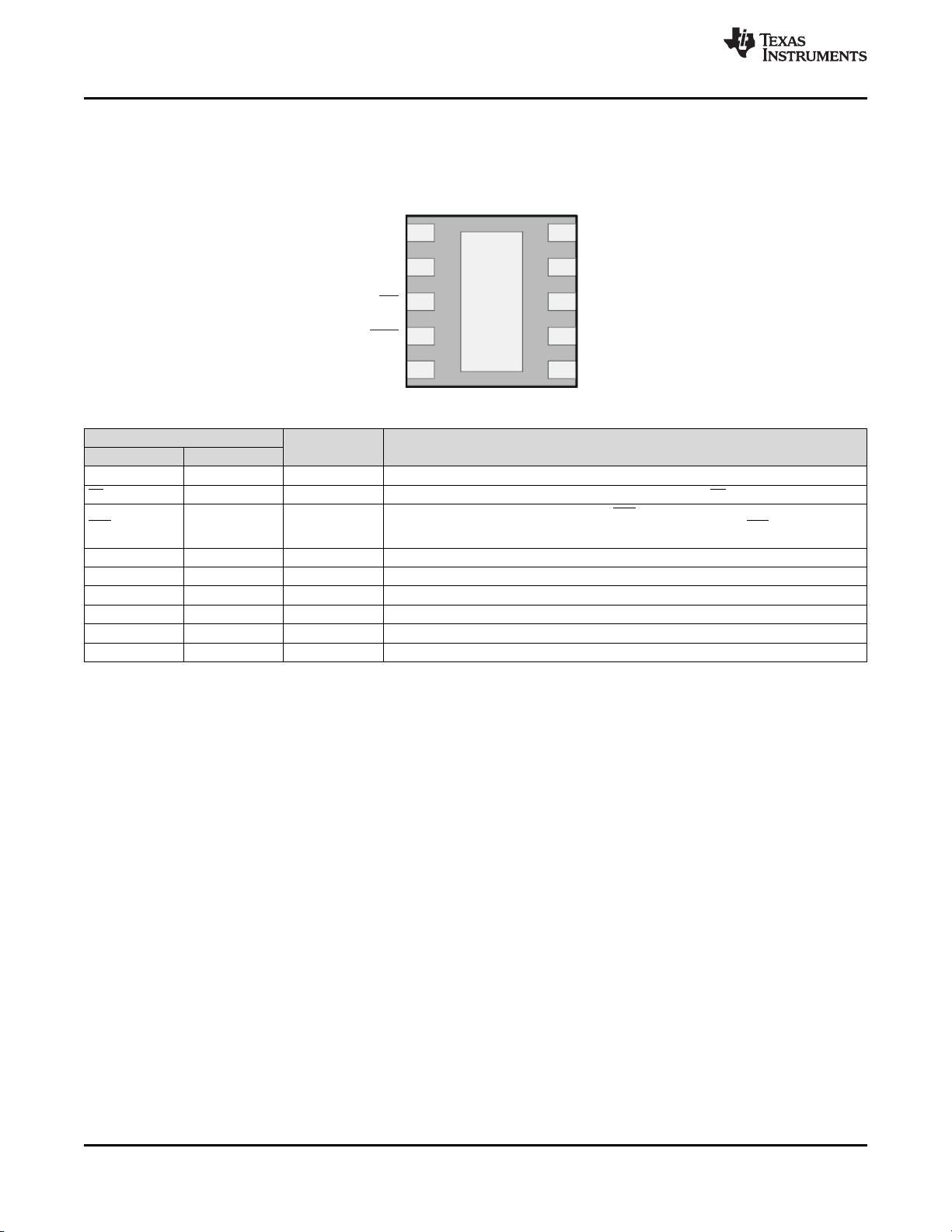
5 Pin Configuration and Functions......................... 4
6 Specifications......................................................... 5
6.1 Absolute Maximum Ratings ...................................... 5
6.2 ESD Ratings.............................................................. 5
6.3 Recommended Operating Conditions....................... 5
6.4 Thermal Information.................................................. 6
6.5 Electrical Characteristics, EN, ACK, D+, D–, ID Pins
................................................................................... 6
6.6 Electrical Characteristics OVP Circuits..................... 7
6.7 Supply Current Consumption.................................... 7
6.8 Thermal Shutdown Feature ...................................... 7
6.9 Typical Characteristics.............................................. 8
7 Detailed Description............................................ 10
7.1 Overview ................................................................. 10
7.2 Functional Block Diagram ....................................... 10
7.3 Feature Description................................................. 10
7.4 Device Functional Modes........................................ 12
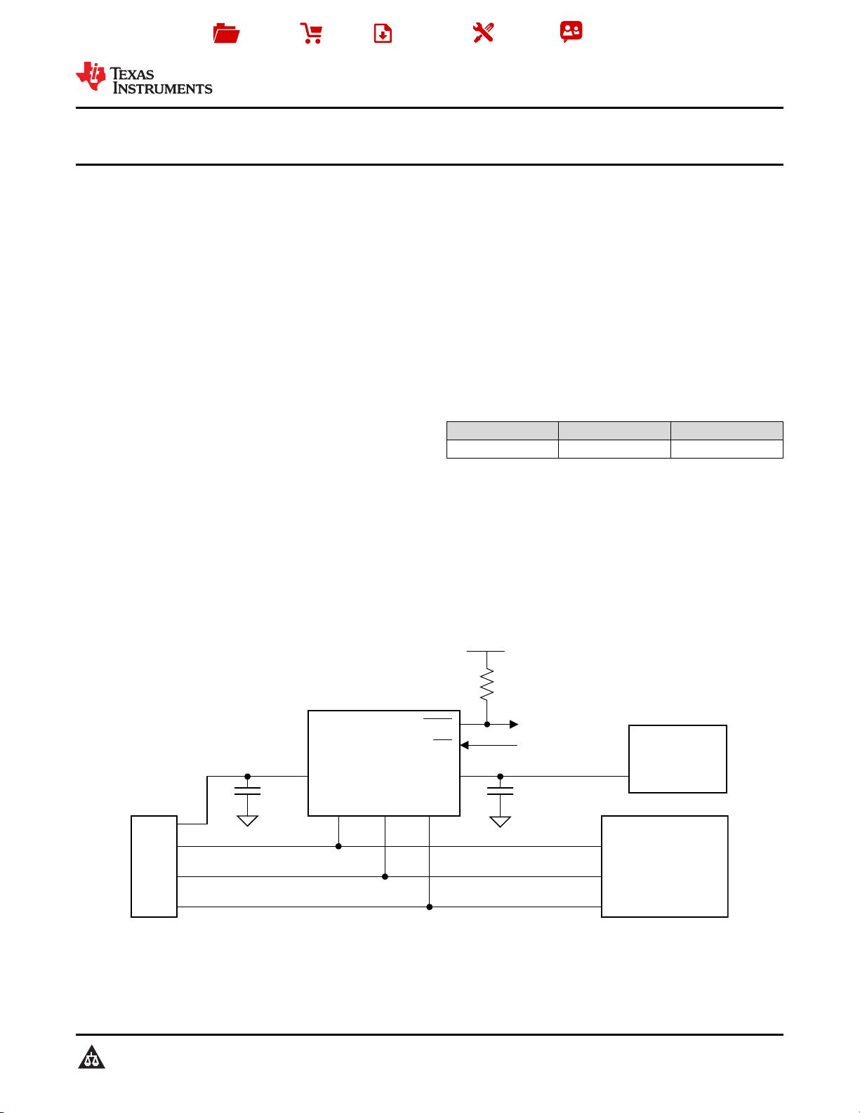
8 Application and Implementation ........................ 13
8.1 Application Information............................................ 13
8.2 Typical Applications ................................................ 13
9 Power Supply Recommendations...................... 16
10 Layout................................................................... 16
10.1 Layout Guidelines ................................................. 16
10.2 Layout Example .................................................... 17
11 器器件件和和文文档档支支持持 ..................................................... 18
11.1 社区资源................................................................ 18
11.2 商标 ....................................................................... 18
11.3 静电放电警告......................................................... 18
11.4 Glossary................................................................ 18
12 机机械械、、封封装装和和可可订订购购信信息息....................................... 18
4 修修订订历历史史记记录录
注:之前版本的页码可能与当前版本有所不同。
Changes from Revision F (September 2015) to Revision G Page
• Added a frequency test condition to capacitance in the Electrical Characteristics table. ..................................................... 6
Changes from Revision E (June 2014) to Revision F Page
• Corrected V
DROP
on nFET under load................................................................................................................................... 10
Changes from Revision D (April 2014) to Revision E Page
• Updated Recommended Operating Conditions table. ........................................................................................................... 5
• Changed terminal name to I
LEAK
from I
L
................................................................................................................................. 6
• Updated Electrical Characteristics OVP Circuits table. .......................................................................................................... 7
• Changed t
ON
MAX value from 18 ms to 22ms ....................................................................................................................... 7
• Changed t
OFF
8 µs value from MAX to TYP............................................................................................................................ 7
• Changed t
d(OVP)
11 µs value from MAX to TYP. ..................................................................................................................... 7
• Changed t
REC
MAX value from 9 ms to 10.5 ms. .................................................................................................................. 7
• Updated Application and Implementation section. .............................................................................................................. 13
Changes from Revision C (December 2011) to Revision D Page
• Added ESD Ratings table....................................................................................................................................................... 5
• Added Recommended Operating Conditions table. ............................................................................................................... 5
• Added Thermal Information table. ......................................................................................................................................... 6
• Updated Electrical Characteristics OVP Circuits table. .......................................................................................................... 7
3
TPD4S014
www.ti.com.cn
ZHCS116G –MAY 2011–REVISED DECEMBER 2015
Copyright © 2011–2015, Texas Instruments Incorporated
Changes from Revision B (October 2011) to Revision C Page
• 已通过更改数据表严格限定了参数,VOP+ 由 5.55V 变更为 5.9V。 ..................................................................................... 1
• 已更新 说明)。...................................................................................................................................................................... 1
Changes from Revision A (June 2011) to Revision B Page
• Changed name of V
CC
to V
BUS
OUT throughout the entire document................................................................................... 10
• Deleted row from Device Operation table. ........................................................................................................................... 12
• Added Eye Diagrams to Typical Characteristics section...................................................................................................... 14
EN
ACK
ID
V
BUS
V
BUS
GND
D+
D-
V OUT
BUS
V OUT
BUS
1
10
6
5
4
TPD4S014
ZHCS116G –MAY 2011–REVISED DECEMBER 2015
www.ti.com.cn
Copyright © 2011–2015, Texas Instruments Incorporated
5 Pin Configuration and Functions
DSQ Package
10-Pin WSON
Top Side/See-Through View
Pin Functions
PIN
TYPE DESCRIPTION
NAME NO.
V
BUS
OUT 1, 2 Power Output Connect to PCB internal PCB plane
EN 3 IO Enable Active-Low Input. Drive EN low to enable the switch. Drive EN high to disable the switch.
ACK 4 I
Open-Drain Adapter-Voltage Indicator Output. ACK is driven low after the VIN voltage is stable
between UVLO and OVLO for 17 ms (typ). Connect a pullup resistor from ACK to the logic I/O
voltage of the host system.
ID 5 IO ESD-protected line
D– 6 IO ESD-protected line
D+ 7 IO ESD-protected line
GND 8 Ground Ground
V
BUS
9, 10 USB Input Power Connector Side of V
BUS
Central PAD Central PAD Heat Sink Electrically disconnected. Use as heat sink. Connect to GND plane via large PCB PAD
5
TPD4S014
www.ti.com.cn
ZHCS116G –MAY 2011–REVISED DECEMBER 2015
Copyright © 2011–2015, Texas Instruments Incorporated
(1) Stresses above these ratings may cause permanent damage. Exposure to absolute maximum conditions for extended periods may
degrade device reliability. These are stress ratings only, and functional operation of the device at these or any other conditions beyond
those specified is not implied.
(2) The algebraic convention, whereby the most negative value is a minimum and the most positive value is a maximum.
6 Specifications
6.1 Absolute Maximum Ratings
over operating free-air temperature range (unless otherwise noted)
(1)(2)
MIN MAX UNIT
Maximum junction temperature –40 150 °C
Max Voltage on V
BUS
–0.5 30 V
Continuous current through nFET 2.6 A
Continuous current through ACK –50 50 mA
Max Current through D+, D–, ID, V
BUS
ESD clamps 50 mA
Max voltage on EN, ACK, D+, D-, ID, V
BUS
OUT 6 V
Storage temperature, T
stg
–65 150 °C
(1) JEDEC document JEP155 states that 500-V HBM allows safe manufacturing with a standard ESD control process. Manufacturing with
less than 500-V HBM is possible with the necessary precautions. Pins listed as ±2000 V may actually have higher performance.
(2) JEDEC document JEP157 states that 250-V CDM allows safe manufacturing with a standard ESD control process. Manufacturing with
less than 250-V CDM is possible with the necessary precautions. Pins listed as ±1000 V may actually have higher performance.
6.2 ESD Ratings
VALUE UNIT
V
(ESD)
Electrostatic discharge
Human-body model (HBM), per ANSI/ESDA/JEDEC JS-001
(1)
±2000
V
Charged-device model (CDM), per JEDEC specification JESD22-C101
(2)
±1000
IEC 61000-4-2 Contact Discharge D+, D–, ID, V
BUS
pins ±1500
IEC 61000-4-2 Air-gap Discharge D+, D–, ID, V
BUS
pins ±1500
(1) IV
BUS
Max value is dependent on ambient temperature. See Thermal Shutdown section.
6.3 Recommended Operating Conditions
over operating free-air temperature range (unless otherwise noted)
MIN NOM MAX UNIT
T
A
Operating free-air temperature –40 85 °C
V
I
Input voltage
V
BUSOUT
–0.1 5.5
V
V
BUS
–0.1 5.5
EN –0.1 5.5
ACK –0.1 5.5
D+, D-, ID, –0.1 5.5
I
VBUS
V
BUS
continuous current
(1)
V
BUS
OUT 2.0 A
C
VBUS
Capacitance on V
BUS
V
BUS
Pin 10 µF
C
VBUS
OUT Capacitance on V
BUS
OUT V
BUS
OUT Pin 10 µF
R
ACK
Pullup resistor on ACK ACK Pin 10 kΩ
剩余24页未读,继续阅读
资源评论
不觉明了
- 粉丝: 3134
- 资源: 5382
上传资源 快速赚钱
- 我的内容管理 展开
- 我的资源 快来上传第一个资源
- 我的收益 登录查看自己的收益
- 我的积分 登录查看自己的积分
- 我的C币 登录后查看C币余额
- 我的收藏
- 我的下载
- 下载帮助
最新资源
- Screenshot_20240509_034911_com.tencent.mtt.jpg
- 基于python实现的医学影像体脂分割+源代码+文档说明(课程设计)
- 基于python实现的医学影像(MIR, CT )图像分割源码+文档说明(高分课程设计)
- 基于python+JavaScript实现的医学影像分割+源代码+文档说明+截图演示+数据(高分毕业设计)
- 基于U-net+pytorch实现的医学影像分割python源码+文档说明+数据+界面截图+博客介绍
- 课程设计-基于Pytorch实现MNIST数据集的手写数字识别源码+数据(Gui界面)+文档说明+模型
- 软件开发国家标准.xls
- pytorch-CNN-SBATM-ubuntudemo
- matplotlibdemo
- pytorch-CNN-dht11温湿度传感器笔记
资源上传下载、课程学习等过程中有任何疑问或建议,欢迎提出宝贵意见哦~我们会及时处理!
点击此处反馈
安全验证
文档复制为VIP权益,开通VIP直接复制
信息提交成功