没有合适的资源?快使用搜索试试~ 我知道了~
TI-LMP90080.pdf
需积分: 10 0 下载量 133 浏览量
2022-12-04
20:46:42
上传
评论 4
收藏 2.1MB PDF 举报
温馨提示
试读
71页
TI-LMP90080.pdf
资源推荐
资源详情
资源评论
LMP90080
IB1
Micro-
Controller
SCLK
VIN0
VIN2
VIN4
VIN6/VREFP2
4-Wire RTD
3-Wire RTD
2 -Wire RTD
1
4
2
3
...
...
VIN7/
VREFN2
CSB
SDO/DRDYB
SDI
D0
D6/DRDYB
...
XOUT
CLK/XIN
GND
VA
IB2
VREFN1
...
VIO
VA
LEDs/
Switches
VREFP1
Thermocouple
+
-
Product Channel Configuration Current Sources
LMP90080 4 Differential/7 Single-Ended Yes
LMP90079 4 Differential/7 Single-Ended No
LMP90078 2 Differential/4 Single-Ended Yes
LMP90077 2 Differential/4 Single-Ended No
LM90xxx 16-bit Sensor AFE Family of Products
Product
Folder
Sample &
Buy
Technical
Documents
Tools &
Software
Support &
Community
An IMPORTANT NOTICE at the end of this data sheet addresses availability, warranty, changes, use in safety-critical applications,
intellectual property matters and other important disclaimers. PRODUCTION DATA.
English Data Sheet: SNAS521
LMP90077
,
LMP90078
,
LMP90079
,
LMP90080
ZHCS587H –JULY 2011–REVISED JANUARY 2016
LMP9007x/LMP90080 传传感感器器 AFE 系系统统::具具有有真真正正连连续续后后台台校校准准功功能能的的多多
通通道道低低功功耗耗 16 位位传传感感器器 AFE
1
1 特特性性
1
• 16 位低功耗 Σ-Δ 模数转换器 (ADC)
• 所有增益上的真连续背景校准
• 使用期望值编程进行适当的系统校准
• 低噪声可编程增益 (1x - 128x)
• 连续后台开路/短路和范围外传感器诊断
• 单周期稳定的 8 个输出数据速率 (ODR)
• 源自 100µA 至 1000 µA 的 2 个已匹配激励电流
(LMP90080/LMP90078)
• 4 个差分输入/7 个单端输入
(LMP90080/LMP90079)
• 2 个差分输入/4 个单端输入
(LMP90078/LMP90077)
• 7 个通用输入/输出引脚
• 用于实现低偏移的斩波稳定缓冲器
• 支持循环冗余码校验 (CRC) 数据链接误差检测的
SPI 4/3 线制接口
• ODR ≤ 13.42SPS 时的 50Hz 至 60Hz 线路扰动抑
制
• 每通道独立增益和 ODR 选择
• 由 WEBENCH
®
传感器 AFE 设计工具提供支持
• 自动通道排序器
• 主主要要技技术术规规范范
– 有效位数 (ENOB)/NFR:高达 16/16 位
– 偏移误差(典型值):8.4nV
– 增益误差(典型值):7ppm
– 总体噪声:< 10µV-rms
– 积分非线性(INL 最大值):±1 最低有效位
(LSB)
– 输出数据速率 (ODR):1.6775 至 214.65SPS
– 模拟电压 V
A
:2.85V 至 5.5V
– 工作温度范围:–40°C 至 125°C
– 封装:28 引脚带外露垫封装
2 应应用用
• 温度和压力发送器
• 应变仪接口
• 工业过程控制
3 说说明明
LLMP9007x 和 LMP90080 是高度集成的多通道低功
耗 16 位传感器模拟前端 (AFE)。此器件特有一个精密
16 位三角积分模数转换器 (ADC),此转换器具有一个
低噪声可编程增益放大器和一个完全差分高阻抗模拟输
入复用器。一个真连续后台校准特性可在所有增益和输
出数据速率上实现校准而又不会中断信号路径。后台校
准特性在温度和时间范围内从根本上消除了增益和偏移
误差,从而在不损失速度和功耗的情况下提供测量精
度。
器器件件信信息息
(1)
器器件件型型号号 封封装装 封封装装尺尺寸寸((标标称称值值))
LMP90077
HTSSOP (28) 9.70mm x 4.40mm
LMP90078
LMP90079
LMP90080
(1) 如需了解所有可用封装,请参见数据表末尾的可订购产品附
录。
典典型型传传感感器器应应用用
2
LMP90077
,
LMP90078
,
LMP90079
,
LMP90080
ZHCS587H –JULY 2011–REVISED JANUARY 2016
www.ti.com.cn
版权 © 2011–2016, Texas Instruments Incorporated
目目录录
1 特特性性.......................................................................... 1
2 应应用用.......................................................................... 1
3 说说明明.......................................................................... 1
4 修修订订历历史史记记录录 ........................................................... 2
5 说说明明 ((续续)).............................................................. 3
6 Device Comparison Table..................................... 3
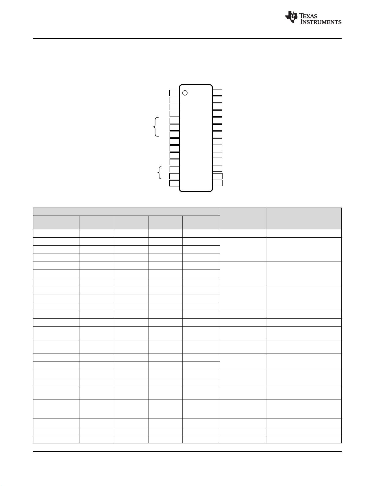
7 Pin Configuration and Functions......................... 4
8 Specifications......................................................... 5
8.1 Absolute Maximum Ratings ...................................... 5
8.2 ESD Ratings.............................................................. 5
8.3 Recommended Operating Conditions....................... 6
8.4 Thermal Information.................................................. 6
8.5 Electrical Characteristics........................................... 6
8.6 Timing Requirements.............................................. 11
8.7 Timing Requirements - CSB Timing ....................... 11
8.8 Timing Requirements - SCLK and SDI Timing ....... 11
8.9 Timing Requirements - SDO Timing With DOD1.... 11
8.10 Timing Requirements - SDO Timing with DOD2 .. 11
8.11 Timing Requirements - SDO and DRDYB Timing 11
8.12 Typical Characteristics.......................................... 15
9 Detailed Description............................................ 20
9.1 Overview ................................................................. 20
9.2 Functional Block Diagram ....................................... 20
9.3 Feature Description................................................. 21
9.4 Device Functional Modes........................................ 29
9.5 Programming........................................................... 32
9.6 Register Maps......................................................... 43
10 Application and Implementation........................ 53
10.1 Application Information.......................................... 53
10.2 Typical Applications .............................................. 54
11 Power Supply Recommendations ..................... 60
12 Layout................................................................... 60
12.1 Layout Guidelines ................................................. 60
12.2 Layout Example .................................................... 60
13 器器件件和和文文档档支支持持 ..................................................... 61
13.1 器件支持................................................................ 61
13.2 相关链接................................................................ 61
13.3 社区资源................................................................ 61
13.4 商标 ....................................................................... 62
13.5 静电放电警告......................................................... 62
13.6 Glossary................................................................ 62
14 机机械械、、封封装装和和可可订订购购信信息息....................................... 62
4 修修订订历历史史记记录录
Changes from Revision G (January 2015) to Revision H Page
• Changed Buffer Enable/Disable. .......................................................................................................................................... 48
• Changed BUF_EN = 1 to 0. ................................................................................................................................................ 53
Changes from Revision F (March 2013) to Revision G Page
• 已添加
引脚配置和功能
部分,ESD
额定值
表,
特性 描述
部分,
器件功能模式
,
应用和实施
部分,
电源相关建议
部
分,
布局
部分,
器件和文档支持
部分以及
机械、封装和可订购信息
部分 ................................................................................ 1
• Added footnote to INL, GE, and Crosstalk specifications. ..................................................................................................... 6
• Changed t
DOD1
specification. ................................................................................................................................................ 11
• Deleted CH_STS and ADC_DOUTM from Compute the CRC... sentence.......................................................................... 38
• Added sentence to the end of the RESET and RESTART section...................................................................................... 39
Changes from Revision E (March 2013) to Revision F Page
• Changed layout of National Data Sheet to TI format ........................................................................................................... 52
3
LMP90077
,
LMP90078
,
LMP90079
,
LMP90080
www.ti.com.cn
ZHCS587H –JULY 2011–REVISED JANUARY 2016
Copyright © 2011–2016, Texas Instruments Incorporated
5 说说明明 ((续续))
LMP9007x 和 LMP90080 的另一项功能是连续后台传感器诊断,无需用户介入即可检测开路和短路状态以及超出
范围的信号,能够强化系统稳定性。
两组独立外部基准引脚可实现多比率测量。此外,LMP90080/LMP90078 还提供两个匹配的可编程电流源,用于为
阻性温度检测器和桥式传感器等外部传感器供电。此外,两种器件还提供了 7 个通用输入/输出 (GPIO) 引脚与外部
发光二极管 (LED) 和开关进行对接,以简化对于绝缘栅的控制。
凭借这一系列 功能, LMP90080/LMP90079/LMP90078/LMP90077 完整模拟前端能够应用于精密的低功耗传感器
应用 例如温度计、压力计、应力计和工业过程控制。LMP90080/LMP90079/LMP90078/LMP90077 采用 28 引脚
外露焊盘封装,均可在 -40°C 至 +125°C 的扩展温度范围内运行。
6 Device Comparison Table
LM90xxx 16-BIT SENOR AFE FAMILY OF PRODUCTS
DEVICE NUMBER CHANNEL CONFIGURATION CURRENT SOURCES
LMP90080
4 Differential/7 Single-Ended
Yes
LMP90079
LMP90078
2 Differential/4 Single-Ended
LMP90077
1
VA
2VIN0
3
VIN1
4
VIN2
5
VIN3
6
VIN4
7
VIN5
8
VREFP1
9
VREFN1
10
VIN6/VREFP2
11
12
28
27
26
25
24
23
22
21
20
19
18
17
VIO
D6 / DRDYB
D5
D4
D3
D2
D1
D0
SDO/DRDYB
SDI
SCLK
13
14
LMP900xx
16
15
VIN7/VREFN2
IB2
IB1
XOUT
CSB
GND
XIN/CLK
LMP90080/
LMP90078 only
LMP90080/
LMP90079 only
4
LMP90077
,
LMP90078
,
LMP90079
,
LMP90080
ZHCS587H –JULY 2011–REVISED JANUARY 2016
www.ti.com.cn
Copyright © 2011–2016, Texas Instruments Incorporated
7 Pin Configuration and Functions
PWP Package
28-Pin HTSSOP
Top View
Pin Functions
PIN
TYPE FUNCTION
NAME
LMP90080
PIN NO.
LMP90079
PIN NO.
LMP90078
PIN NO.
LMP90077 PIN
NO.
VA 1 1 1 1 Analog Supply Analog power supply pin
VIN0 2 2 2 2
Analog Input Analog input pinsVIN1 3 3 3 3
VIN2 4 4 4 4
VIN3 5 5 — —
Analog Input Analog input pinsVIN4 6 6 — —
VIN5 7 7 — —
VIN3 — — 5 5
No Connect
No connect: must be left
unconnected
VIN4 — — 6 6
VIN5 — — 7 7
VREFP1 8 8 8 8 Analog Input Positive reference input
VREFN1 9 9 9 9 Analog Input Negative reference input
VIN6 / VREFP2 10 10 10 10 Analog Input
Analog input pin or VREFP2
input
VIN7 / VREFN2 11 11 11 11 Analog Input
Analog input pin or VREFN2
input
IB2 12 — 12 —
Analog output
Excitation current sources for
external RTDs
IB1 13 — 13 —
IB2 — 12 — 12
No Connect
No connect: must be left
unconnected
IB1 — 13 — 13
XOUT 14 14 14 14 Analog output
External crystal oscillator
connection
XIN / CLK 15 15 15 15 Analog input
External crystal oscillator
connection or external clock
input
GND 16 16 16 16 Ground Power supply ground
CSB 17 17 17 17 Digital Input Chip select bar
SCLK 18 18 18 18 Digital Input Serial clock
5
LMP90077
,
LMP90078
,
LMP90079
,
LMP90080
www.ti.com.cn
ZHCS587H –JULY 2011–REVISED JANUARY 2016
Copyright © 2011–2016, Texas Instruments Incorporated
Pin Functions (continued)
PIN
TYPE FUNCTION
NAME
LMP90080
PIN NO.
LMP90079
PIN NO.
LMP90078
PIN NO.
LMP90077 PIN
NO.
SDI 19 19 19 19 Digital Input Serial data input
SDO / DRDYB 20 20 20 20 Digital Output
Serial data output and data
ready bar
D0 21 21 21 21
Digital IO
General purpose input/output
(GPIO) pins
D1 22 22 22 22
D2 23 23 23 23
D3 24 24 24 24
D4 25 25 25 25
D5 26 26 26 26
D6 / DRDYB 27 27 27 27 Digital IO
General purpose input/output
pin or data ready bar
VIO 28 28 28 28 Digital Supply Digital input/output supply pin
Thermal Pad — — — — — Leave the thermal pad floating
(1) All voltages are measured with respect to GND, unless otherwise specified
(2) Stresses beyond those listed under Absolute Maximum Ratings may cause permanent damage to the device. These are stress ratings
only, which do not imply functional operation of the device at these or any other conditions beyond those indicated under Recommended
Operating Conditions. Exposure to absolute-maximum-rated conditions for extended periods may affect device reliability.
(3) For soldering specifications see product folder at http://www.ti.com and http://www.ti.com/lit/SNOA549
(4) If Military/Aerospace specified devices are required, contact the Texas Instruments Sales Office/ Distributors for availability and
specifications.
(5) When the input voltage (VIN) exceeds the power supply (VIN < GND or VIN > VA), the current at that pin must be limited to 5mA and
VIN has to be within the Absolute Maximum Rating for that pin. The 20 mA package input current rating limits the number of pins that
can safely exceed the power supplies with current flow to four pins.
8 Specifications
8.1 Absolute Maximum Ratings
See
(1)(2)(3)(4)
.
MIN MAX UNIT
Analog Supply Voltage, VA –0.3 6.0
V
Digital I/O Supply Voltage, VIO –0.3 6.0
Reference Voltage, VREF –0.3 VA+0.3
Voltage on Any Analog Input Pin to GND
(5)
–0.3 VA+0.3
Voltage on Any Digital Input PIN to GND
(5)
–0.3 VIO+0.3
Voltage on SDO
(5)
–0.3 VIO+0.3
Input Current at Any Pin
(5)
5
mAOutput Current Source or Sink by SDO 5
Total Package Input and Output Current 20
Junction Temperature (T
JMAX
) 150 °C
Storage Temperature (T
stg
) –65 150 °C
(1) JEDEC document JEP155 states that 500-V HBM allows safe manufacturing with a standard ESD control process.
(2) JEDEC document JEP157 states that 250-V CDM allows safe manufacturing with a standard ESD control process.
8.2 ESD Ratings
VALUE UNIT
V
(ESD)
Electrostatic discharge
Human-body model (HBM), per ANSI/ESDA/JEDEC JS-001
(1)
±2500
V
Charged-device model (CDM), per JEDEC specification JESD22-
C101
(2)
±1250
Machine models (MM) ±200
剩余70页未读,继续阅读
资源评论
不觉明了
- 粉丝: 3118
- 资源: 5348
上传资源 快速赚钱
- 我的内容管理 展开
- 我的资源 快来上传第一个资源
- 我的收益 登录查看自己的收益
- 我的积分 登录查看自己的积分
- 我的C币 登录后查看C币余额
- 我的收藏
- 我的下载
- 下载帮助
安全验证
文档复制为VIP权益,开通VIP直接复制
信息提交成功