没有合适的资源?快使用搜索试试~ 我知道了~
TI-LMP92001.pdf
需积分: 10 0 下载量 108 浏览量
2022-11-27
16:41:30
上传
评论 4
收藏 1.23MB PDF 举报
温馨提示
试读
40页
TI-LMP92001.pdf
资源推荐
资源详情
资源评论
LMP92001
www.ti.com
SNAS507B –FEBRUARY 2011–REVISED APRIL 2012
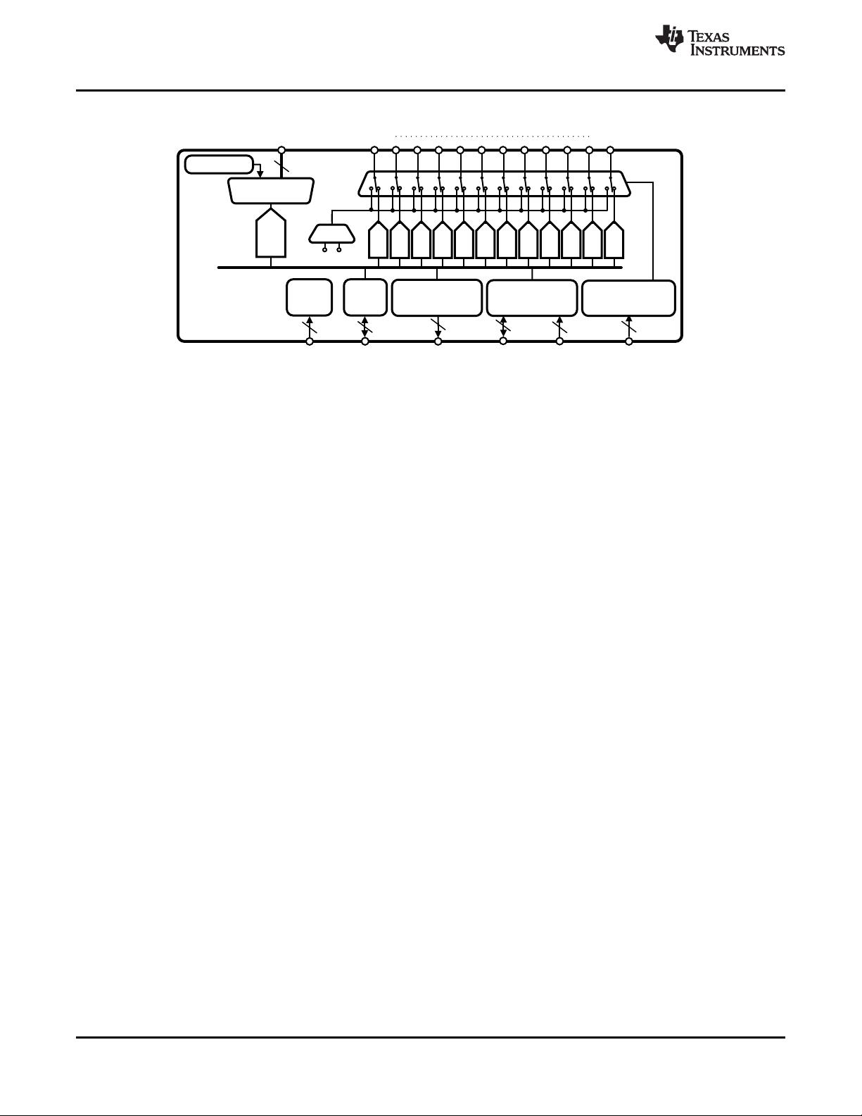
LMP92001 Analog System Monitor and Controller
Check for Samples: LMP92001
1
FEATURES
APPLICATIONS
2
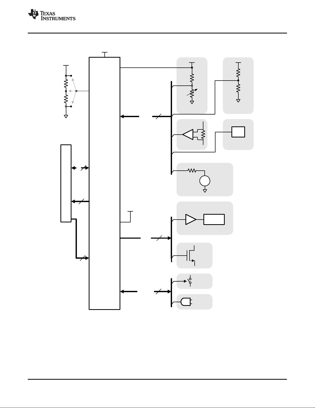
• 16 Analog Voltage Monitoring Channels
• RF PA Bias Monitoring and Control
– 12-bit ADC with Programmable Input MUX • System Monitoring and Control
– No Missing Codes • Industrial Monitoring and Control
– Total Unadjusted Error (TUE) ±0.1% • Test Equipment and Instrumentation
– Single-Shot or Continuous Conversion
DESCRIPTION
Modes
The LMP92001 is a complete analog monitoring and
– Programmable Window Comparator
control circuit which includes a sixteen channel 12-bit
Function
Analog to Digital Converter (ADC), twelve 12-bit
– Interrupt Signal Generation for Input Out-of-
Digital to Analog Converters (DACs), an internal
Bound Condition
reference, an internal temp sensor, an 8-bit GPIO
port, and an I
2
C-compatible interface.
• 12 Programmable Analog Voltage Outputs
– Twelve 12-bit DACs
The ADC can be used to monitor rail voltages,
current sense amplifier outputs or sensors and
– Specified Monotonic
includes a programmable window comparator
– Settling Time 8.5 µs
function on six of its 16 channels to detect out-of
– Simultaneous Update of All Channels to
range conditions.
Same Value
The DACs can be used to control PA bias points,
– Asynchronous Output Control Forces Rail
actuators, potentiometers, etc. When required, the
Voltage at Output
outputs can be instantaneously driven to either supply
rail using the output switches and the asynchronous
• Voltage Reference
DAC control inputs.
– User-Selectable Source: External or Internal
Both ADC and DACs can use either the internal 4.5V
– Internal Reference 4.5V ±0.7%
reference or an external reference independently.
• Analog Temperature Sensor
The built-in temperature sensor is treated as the 17th
– Readable via ADC Channel 17
analog sense input. In addition, the 8-bit GPIO port
– Temperature Error ±2°C
allows for the resources of the microcontroller to be
• 8-bit GPIO Port
further extended, providing even more flexibility.
– Each Bit Individually Programmable
The LMP92001 is available in a space saving 54-pin
• I
2
C-Compatible Bus
WQFN package and is operational over the full −
40°C to 125°C temperature range.
– Supports Standard and Fast Modes
– Bus TIMEOUT Function
– Supports Block Data Transfers
1
Please be aware that an important notice concerning availability, standard warranty, and use in critical applications of
Texas Instruments semiconductor products and disclaimers thereto appears at the end of this data sheet.
2All trademarks are the property of their respective owners.
PRODUCTION DATA information is current as of publication date.
Copyright © 2011–2012, Texas Instruments Incorporated
Products conform to specifications per the terms of the Texas
Instruments standard warranty. Production processing does not
necessarily include testing of all parameters.
Multiplexer
ADC
LMP92001
16
Temp. Sensor
GNDVDD
DAC
DAC
DAC
DAC
DAC
DAC
DAC
DAC
DAC
DAC
DAC
DAC
Int/Ext
Ref
2
2
I
2
C
Interface
2
Interrupt Status &
Control
8
GPIO
4
Asynchronous DAC
Control
AREF
DREF
GPIO[7:0]
INT[2:1]
SCL
SDA
C[4:1]
OUT12
OUT1
IN[16:1]
2
AS[1:0]
LMP92001
SNAS507B –FEBRUARY 2011–REVISED APRIL 2012
www.ti.com
Block Diagram
2 Submit Documentation Feedback Copyright © 2011–2012, Texas Instruments Incorporated
Product Folder Links: LMP92001
LMP92001
µC
Temp
IN[16:1]
Voltage
Sense
Channels
AREF
Ratiometric
Sensing
Scaled
Voltage
Sensing
Current
sensing
Analog
Sensors
I
2
C
LMP8640
LM94023
+
-
ROUT<10k
16
Servo
OUT[12:1]
Actuator
Control
PA
Bias
Control
GPIO[7:0]
8
Bidirectional
Digital Bus
Digital
Control
Digital
Status
Indicators
12
INT[2:1]
2
SCL, SDA
4
VDD
C[4:1]
5V
5V
48V
DREF
5V
2
Voltage
Source
AS[1:0]
5V
Analog
Voltage
Control
LMP92001
www.ti.com
SNAS507B –FEBRUARY 2011–REVISED APRIL 2012
Typical Application
Overview
The LMP92001 has a flexible, feature-rich functionality which makes it ideally suited for many analog monitoring
and control applications, for example base-station PA subsystems. This device provides the analog interface
between a programmable supervisor, such as a microcontroller, and an analog system whose behavior is to be
monitored and controlled by the supervisor.
To facilitate analog monitoring functionality, the device contains a single 12-bit ADC fronted by a 17-input
multiplexor. The 16 MUX inputs are available to the user via pins IN[16:1]. The last remaining MUX channel is
reserved for the internal analog temperature sensor.
Copyright © 2011–2012, Texas Instruments Incorporated Submit Documentation Feedback 3
Product Folder Links: LMP92001
LMP92001
SNAS507B –FEBRUARY 2011–REVISED APRIL 2012
www.ti.com
The analog control functionality is served by twelve 12-bit voltage output DACs. Besides producing voltage
corresponding to the digital input code, the DACs can be forced by the user to either rail instantaneously.
Additional digital monitoring and control can be realized via the General Purpose I/O port GPIO[7:0].
Two more blocks are present for added functionality: a local temperature sensor (already mentioned above) and
an internal reference voltage generator.
17-CHANNEL ANALOG SENSE WITH 12-BIT ADC
The user can monitor up to 16 external voltages with the 12-bit ADC and its 17-channel input MUX. Typically
these voltages will be generated by the analog sensors, instrumentation amplifiers, current sense amplifiers, or
simply resistive dividers if high potentials need to be measured. Channel 17 of the input MUX is reserved for the
internal temperature sensor, and is not available as an external input to the device.
User can program which MUX channels to enable, and whether to convert these channel inputs in sequence
continuously, or in a single-shot mode. Upon completion all conversion results are stored in the internal data
registers, and can be read back by the user via the I
2
C-compatible interface.
Analog input channels 1-3 and 9-11 have a built-in digital window comparator function with user programmable
thresholds. This function can be used to alert the supervisor microcontroller of an out-of-bound condition. The
comparator function result is stored in the internal status register which is user accessible. It can also be used as
the interrupt signal generator where the out of bound conditions will be reported via the INT[2:1] output pins.
Sequencing of the analog sense system is governed by the internal controller. Once enabled the MUX, the ADC,
the window comparator and the interrupts perform their function without further user intervention.
PROGRAMMABLE ANALOG CONTROL VOLTAGE OUTPUTS
Twelve identical individually programmable 12-bit DAC blocks are available to generate analog voltages, which
can be used to control bias conditions of external circuits, position of servos, etc.
In case simultaneous update of all outputs to the same level is needed, a single internal register is provided that
effects simultaneous update of all DAC data registers.
A DAC, by definition, produces an output in the range of GND to DREF. In some systems, however, it may be
desirable for the OUT pins to produce either GND or VDD, i.e., beyond DREF. This is made possible via the
asynchronous DAC control inputs C[4:1]. When activated, these inputs will force the OUT pins to either rail. The
choice of rail is made in the internal control register.
INTERNAL ANALOG TEMPERATURE SENSOR
An on-board analog temperature sensor is available to monitor the device’s own temperature. Once enabled, the
analog temperature sensor output is sampled via the MUX channel 17, and its conversion result is stored in the
internal register for user read back.
INTERNAL VOLTAGE REFERENCE SOURCE
Another resource available to the user is the internal, temperature-compensated reference voltage source. By
default both ADC and DACs expect reference potentials to be supplied externally. The user can choose to
enable the internal reference and use it with the ADC and/or the DACs.
The internal reference source cannot drive an external load.
8-BIT GENERAL PURPOSE I/O
The GPIO port can be used to expand the microcontroller capabilities. This port is memory mapped to the
internal register, which in turn is accessible via the I
2
C-compatible interface. Since each bit is individually
programmable as an Input or Output, the port is ideally suited for external switch control and status flag
monitoring, without further burdening of microcontroller I/O resources.
I
2
C-COMPATIBLE INTERFACE
The microcontroller supervisor communicates with LMP92001 via a popular I
2
C-compatible 2–wire interface. This
interface provides the user full access to all Data, Status and Control registers of the device.
4 Submit Documentation Feedback Copyright © 2011–2012, Texas Instruments Incorporated
Product Folder Links: LMP92001
8
7
6
5
4
3
2
1
16
15
14
13
12
11
10
9
18
17
53
52
51
50
49
48
47
46
54
20
21
22
23
24
25
26
27
19
38
39
40
41
42
43
44
45
30
31
32
33
34
35
36
37
28
29
IN4
IN3
IN2
IN1
GND
OUT6
OUT5
OUT4
GPIO1
GPIO0
VDD
GND
IN8
IN7
IN6
IN5
GPIO3
GPIO2
IN11
IN10
IN9
GND
OUT12
OUT11
OUT10
GND
C4
AS0
AS1
IN16
IN15
IN14
IN13
IN12
C2
C3
GPIO5
GPIO6
GPIO7
SCL
SDA
INT1
INT2
C1
GPIO4
OUT2
OUT1
DREF
VDD
AREF
OUT7
OUT8
OUT9
OUT3
DAP
LMP92001
www.ti.com
SNAS507B –FEBRUARY 2011–REVISED APRIL 2012
There are 2 address setting pins, AS[1:0], that allow the device to occupy any one of 9 possible Interface
Addresses on the bus.
Block Access commands are provided to minimize the transfer overhead of larger data sets.
Connection Diagram
Figure 1. WQFN-54 (NJY0054A)
Top View
Copyright © 2011–2012, Texas Instruments Incorporated Submit Documentation Feedback 5
Product Folder Links: LMP92001
剩余39页未读,继续阅读
资源评论
不觉明了
- 粉丝: 3164
- 资源: 5429
上传资源 快速赚钱
- 我的内容管理 展开
- 我的资源 快来上传第一个资源
- 我的收益 登录查看自己的收益
- 我的积分 登录查看自己的积分
- 我的C币 登录后查看C币余额
- 我的收藏
- 我的下载
- 下载帮助
安全验证
文档复制为VIP权益,开通VIP直接复制
信息提交成功