没有合适的资源?快使用搜索试试~ 我知道了~
TI-UCC24636.pdf
需积分: 8 0 下载量 41 浏览量
2022-10-26
23:20:07
上传
评论 5
收藏 2.4MB PDF 举报
温馨提示
试读
36页
TI-UCC24636.pdf
资源详情
资源评论
资源推荐
Gate Drive
1-mŸ R
DSON
MOSFET Example
UCC24636
Secondary
Current
Gate Drive
VDS Sensing
Driver
5 A
300 ns
15 A
5 Ps
0.85 A
+
±
DRV
CS
VDD
GND
VS
VAC
FB
UCC28740
C
OUT
C
B2
C
B1
HV
TL431
V
OUT
N
S
UCC24636
VPC
DRV
GND
TBLK
VSC
VDD
R
VPC1
R
VPC2
R
VSC1
R
VSC2
R
TBLK
5
1
4
6
2
3
N
P
Product
Folder
Sample &
Buy
Technical
Documents
Tools &
Software
Support &
Community
Reference
Design
An IMPORTANT NOTICE at the end of this data sheet addresses availability, warranty, changes, use in safety-critical applications,
intellectual property matters and other important disclaimers. PRODUCTION DATA.
English Data Sheet: SLUSCG2
UCC24636
ZHCSES5A –MARCH 2016–REVISED MARCH 2016
UCC24636 具具有有超超低低待待机机电电流流
的的同同步步整整流流器器 (SR) 控控制制器器
1
1 特特性性
1
• 针对 5V 至 24V 输出断续/转换模式反激转换器而优
化的二次侧 SR 控制器
• 通过伏秒平衡控制实现最高整流器效率
• 兼容一次侧同步整流器 (PSR) 和二次侧同步整流器
(SSR) 反激控制器
• 110µA 超低待机电流消耗
• 通过自动检测待机模式禁用 SR 开关以降低无负载
时的功耗
• SR 关断与 R
DSON
和寄生电感无关
• 工作频率高达 130kHz
• 宽 VDD 范围:3.6V 至 28V
• 自适应栅极驱动钳位
• 开路和短路引脚故障保护
2 应应用用
• 智能手机和平板电脑的 AC/DC 适配器
• 带有 Type-C 连接器的 USB 充电器
• 笔记本电脑和超极本适配器
• 工业用开关模式电源 (SMPS) 中的高效率反激转换
器
• 服务器和台式机中的高效率辅助电源 应用
3 说说明明
UCC24636 SR 是一款紧凑型 6 引脚二次侧同步整流
器 MOSFET 控制器和驱动器,适用于在断续 (DCM)
和转换模式 (TM) 下工作的高效率反激转换器。与测量
SR MOSFET 漏极电压的传统 SR 控制器不同的
是,UCC24636 采用伏秒平衡控制方案来确定 SR
MOSFET 的关闭转换;因此,SR 导通时间与
MOSFET R
DSON
、寄生电感或振铃无关,这在组件选
择和 PCB 布局布线方面给予了设计人员更大的灵活
性。该控制方法可为给定的 MOSFET 实现最长的 SR
导通时间和最高的整流器效率。
该控制器内置智能特性,可在检测到转换器中无负载运
行时自动进入待机模式。在待机模式下,它会禁用 SR
MOSFET 并将其偏置电源电流降至 110uA,从而进一
步降低总体系统待机功耗。该控制器具有较宽的 VDD
工作电压范围,允许直接从控制器输出获取偏置电压以
实现输出电压固定或可变的设计。这消除了主变压器对
辅助绕组的需求,从而简化电路设计并降低成本。
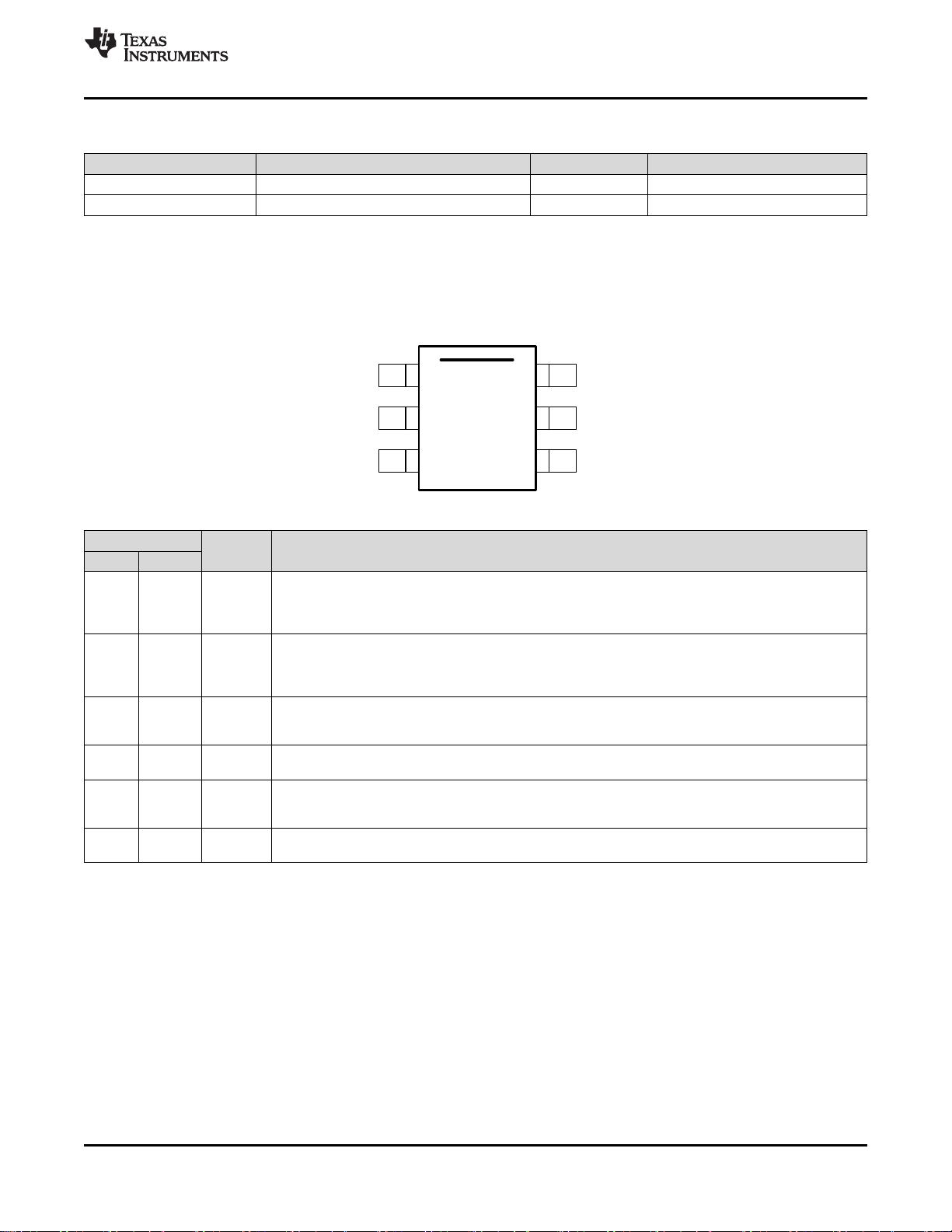
器器件件信信息息
(1)
器器件件型型号号 封封装装 封封装装尺尺寸寸((标标称称值值))
UCC24636 SOT23 (6) 2.92mm x 1.30mm
(1) 要了解所有可用封装,请见数据表末尾的可订购产品附录。
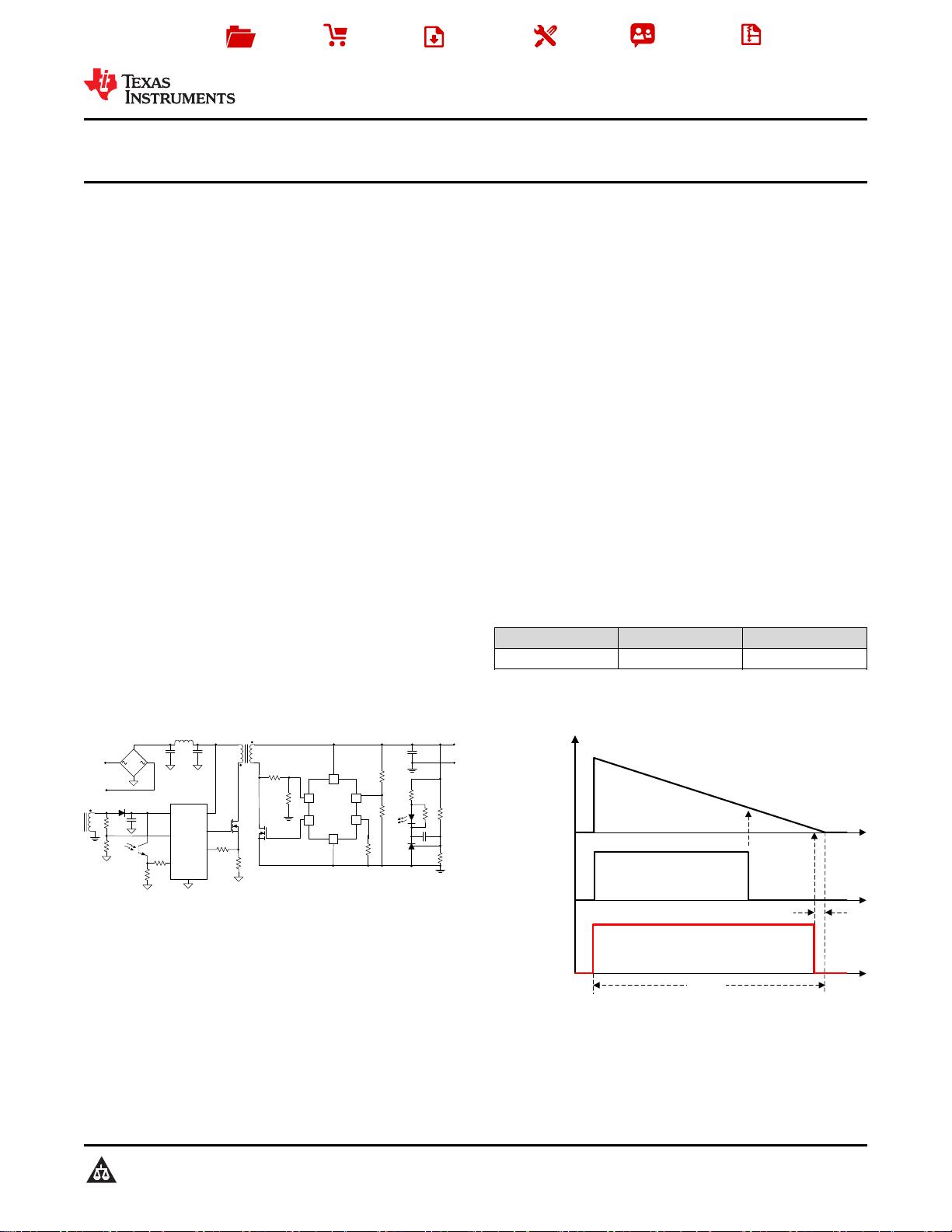
简简化化电电路路原原理理图图 栅栅极极驱驱动动时时序序与与 VDS 感感测测 SR 驱驱动动器器间间的的关关系系
2
UCC24636
ZHCSES5A –MARCH 2016–REVISED MARCH 2016
www.ti.com.cn
Copyright © 2016, Texas Instruments Incorporated
目目录录
1 特特性性.......................................................................... 1
2 应应用用.......................................................................... 1
3 说说明明.......................................................................... 1
4 修修订订历历史史记记录录 ........................................................... 2
5 Device Comparison Table..................................... 3
6 Pin Configuration and Functions......................... 3
7 Specifications......................................................... 4
7.1 Absolute Maximum Ratings ...................................... 4
7.2 ESD Ratings.............................................................. 4
7.3 Recommended Operating Conditions....................... 4
7.4 Thermal Information.................................................. 4
7.5 Electrical Characteristics........................................... 5
7.6 Timing Requirements ............................................... 6
7.7 Typical Characteristics.............................................. 7
8 Detailed Description.............................................. 9
8.1 Overview ................................................................... 9
8.2 Functional Block Diagram ......................................... 9
8.3 Feature Description................................................. 10
8.4 Device Functional Modes........................................ 19
9 Application and Implementation ........................ 20
9.1 Application Information............................................ 20
9.2 Typical Application ................................................. 20
9.3 Do's and Don'ts ...................................................... 27
10 Power Supply Recommendations ..................... 27
11 Layout................................................................... 28
11.1 Layout Guidelines ................................................. 28
11.2 Layout Example .................................................... 29
12 器器件件和和文文档档支支持持 ..................................................... 30
12.1 器件支持 ............................................................... 30
12.2 文档支持................................................................ 30
12.3 商标 ....................................................................... 30
12.4 静电放电警告......................................................... 30
12.5 Glossary................................................................ 30
13 机机械械、、封封装装和和可可订订购购信信息息....................................... 30
4 修修订订历历史史记记录录
注:之前版本的页码可能与当前版本有所不同。
Changes from Original (December 2015) to Revision A Page
• 已将器件状态从“产品预览”更改为“量产数据”并已发布完整数据表。 ...................................................................................... 1
1
2
3 4
5
6
DRV
GND
VPC
TBLK
VSC
VDD
1
2
3
4
5
6
3
UCC24636
www.ti.com.cn
ZHCSES5A –MARCH 2016–REVISED MARCH 2016
Copyright © 2016, Texas Instruments Incorporated
5 Device Comparison Table
PART NUMBER CCM DEAD TIME CONTROL t
OFF
(µs) F
SW(MAX)
(kHz)
UCC24636 No 4.35 130
UCC24630 Yes 2.5 200
(1) P = Power, G = Ground, I = Input, O = Output, I/O = Input/Output
6 Pin Configuration and Functions
DBV Package
6-Pin SOT23
Top View
Pin Functions
PIN
I/O
(1)
DESCRIPTION
NO. NAME
1 VPC I
The Voltage during Primary Conduction pin is connected to a resistor divider from the SR MOSFET
drain. This pin determines a sample of the primary-side MOSFET volt seconds during the primary on-
time. This voltage programs a voltage controlled current source for the internal VPC ramp charging
current.
2 VSC I
The Voltage during Secondary Conduction pin is connected to a resistor divider from the power-supply
output. This pin determines a sample of the secondary-side output voltage used to determine SR
MOSFET conduction time. This voltage programs a voltage controlled current source for the internal VSC
ramp charging current.
3 TBLK –
TIME BLANK pin is used to select the blanking time of the VPC rising edge. A programmable range from
200 ns to 2 µs is available to prevent false detection of the primary on-time due to ringing during DCM
operation.
4 DRV O
DRIVE is an output used to drive the gate of an external synchronous rectifier N-channel MOSFET
switching transistor, with source pin connected to GND.
5 GND G
The GROUND pin is both the reference pin for the controller and the low-side return for the drive output.
Special care should be taken to return all AC decoupling capacitors as close as possible to this pin and
avoid any common trace length with analog signal return paths.
6 VDD P
VDD is the bias supply input pin to the controller. A carefully placed bypass capacitor to GND is required
on this pin.
4
UCC24636
ZHCSES5A –MARCH 2016–REVISED MARCH 2016
www.ti.com.cn
Copyright © 2016, Texas Instruments Incorporated
(1) Stresses beyond those listed under Absolute Maximum Ratings may cause permanent damage to the device. These are stress ratings
only, which do not imply functional operation of the device at these or any other conditions beyond those indicated under Recommended
Operating Conditions. Exposure to absolute-maximum-rated conditions for extended periods may affect device reliability.
7 Specifications
7.1 Absolute Maximum Ratings
over operating free-air temperature range (unless otherwise noted)
(1)
MIN MAX UNIT
V
VDD
Bias supply voltage, VDD –0.3 30 V
I
DRV
Continuous gate current sink, DRV 50 mA
I
DRV
Continuous gate current source, DRV –50 mA
I
VPC
Peak VPC pin current –1.2 mA
V
DRV
Gate drive voltage at DRV –0.3 Self-limiting V
V
VPC
, V
VSC
Voltage range, VPC, VSC –0.3 4.5 V
T
J
Operating junction temperature range –55 150 °C
T
L
Lead temperature 0.6 mm from case for 10 seconds 260 °C
T
stg
Storage temperature –65 150 °C
(1) JEDEC document JEP155 states that 2000-V HBM allows safe manufacturing with a standard ESD control process. Pins listed as
±2000 V may actually have higher performance.
(2) JEDEC document JEP157 states that 500-V CDM allows safe manufacturing with a standard ESD control process. Pins listed as ±500 V
may actually have higher performance.
7.2 ESD Ratings
VALUE UNIT
V
(ESD)
Electrostatic
discharge
Human-body model (HBM), per ANSI/ESDA/JEDEC JS-001
(1)
±2000
V
Charged-device model (CDM), per JEDEC specification JESD22-C101
(2)
±500
7.3 Recommended Operating Conditions
over operating free-air temperature range (unless otherwise noted)
MIN MAX UNIT
V
VDD
Bias supply operating voltage 3.75 28 V
C
VDD
VDD bypass capacitor 0.22 µF
T
J
Operating junction temperature -40 125 °C
V
VPC
, V
VSC
Operating range –0.3 2.2 V
(1) For more information about traditional and new thermal metrics, see the Semiconductor and IC Package Thermal Metrics application
report, SPRA953.
7.4 Thermal Information
THERMAL METRIC
(1)
UCC24636
UNITDBV (SOT23)
6 PINS
R
θJA
Junction-to-ambient thermal resistance 180 °C/W
R
θJC(top)
Junction-to-case (top) thermal resistance 71.2 °C/W
R
θJB
Junction-to-board thermal resistance 44 °C/W
ψ
JT
Junction-to-top characterization parameter 5.1 °C/W
ψ
JB
Junction-to-board characterization parameter 13.8 °C/W
5
UCC24636
www.ti.com.cn
ZHCSES5A –MARCH 2016–REVISED MARCH 2016
Copyright © 2016, Texas Instruments Incorporated
7.5 Electrical Characteristics
over operating free-air temperature, VDD = 12 V, T
A
= –40°C to 125°C, T
A
= T
J
(unless otherwise noted)
PARAMETER TEST CONDITION MIN TYP MAX UNIT
SUPPLY INPUT
I
RUN
Supply current, run I
DRV
= 0, run state, F
SW
= 0 kHz 0.9 1.2 mA
I
STBY
Supply current, standby I
DRV
= 0, standby mode 110 160 µA
UNDER-VOLTAGE LOCKOUT
V
VDD(on)
VDD turn-on threshold V
VDD
low to high 3.9 4 4.3 V
V
VDD(off)
VDD turn-off threshold V
VDD
high to low 3.3 3.6 3.7 V
DRV
R
DRVLS
DRV low-side drive resistance I
DRV
= 100 mA 1 2 Ω
V
DRVST
DRV pull down in start-up V
DD
= 0 to 2 V, I
DRV
= 10 µA 0.95 V
V
DRCL
DRV clamp voltage V
VDD
= 30 V 11 13 15 V
V
PMOS
Disable PMOS high-side drive
V
DD
voltage to disable rail-to-rail
drive, V
DD
rising
9.3 10 10.5 V
V
PMOS-HYS
PMOS enable hysteresis
V
DD
voltage hysteresis to enable rail
to rail drive, V
DD
falling
0.75 1 1.25 V
V
DRHI
DRV pull-up high voltage V
VDD
= 5 V, I
DRV
= 15 mA 4.6 4.75 5 V
VSC INPUT
V
VSCEN
SR enable voltage V
VSC
> V
VSCEN
, V
VSC
rising 250 300 340 mV
V
VSC-HYS
SR enable hysteresis V
VSC
falling 50 mV
V
VSCDIS
SR disable voltage 220 250 280 mV
I
VSC
Input bias current V
VSC
= 2 V –0.25 0 0.4 µA
VPC INPUT
V
VPCEN
SR enable voltage V
VPCEN
< V
VPC
345 400 450 mV
V
VPCDIS
VPC threshold to disable SR V
VPC
> V
VPCDIS
2.6 2.85 3.1 V
V
VPC-TH
Threshold of V
VPC
rising edge
V
VPC
= 0.95 V, V
VPC-TH
= 0.85 x V
VPC
previous cycle
0.76 0.808 0.86 V
V
VPC-TH-CLP
Clamp threshold of V
VPC
rising edge V
VPC
= 2 V 0.9 1 1.1 V
I
VPC
Input bias current V
VPC
= 2 V –0.25 0 0.4 µA
CURRENT EMULATOR
Ratio
VPC_VSC
K
VPC
/K
VSC
V
VPC
= 1.25 V, t
VPC
= 1 µs,
V
VSC
= 1.25 V
3.97 4.17 4.35
V
VPC
= 1.25 V, t
VPC
= 5 µs,
V
VSC
= 1.25 V
3.95 4.17 4.37
V
VPC
= 2 V, t
VPC
= 1 µs,
V
VSC
= 1.25 V
3.85 4.09 4.26
V
VPC
= 1.25 V, t
VPC
= 1 µs,
V
VSC
= 0.45 V
3.85 4.07 4.28
剩余35页未读,继续阅读
不觉明了
- 粉丝: 3117
- 资源: 5348
上传资源 快速赚钱
- 我的内容管理 展开
- 我的资源 快来上传第一个资源
- 我的收益 登录查看自己的收益
- 我的积分 登录查看自己的积分
- 我的C币 登录后查看C币余额
- 我的收藏
- 我的下载
- 下载帮助
安全验证
文档复制为VIP权益,开通VIP直接复制
信息提交成功
评论0