没有合适的资源?快使用搜索试试~ 我知道了~
TI-UCC3974.pdf
需积分: 10 0 下载量 197 浏览量
2022-11-19
23:38:16
上传
评论 5
收藏 224KB PDF 举报
温馨提示
试读
14页
TI-UCC3974.pdf
资源推荐
资源详情
资源评论
SLUS485A – JULY 2001 – REVISED NOVEMBER 2001
1
www.ti.com
FEATURES
D
Synchronous or Nonsynchronous Operation
D Dual Output and Control Stages
D BiCMOS Technology
D Accurate Current Control with 2-mA Typical
Supply Current
D Analog or Digital Low-Frequency Dimming
Capability
D Open Lamp Protection with Voltage Clamp
D 4.5-V to 25-V Operation
D PWM Frequencies Synchronized to External
Resonant Tanks
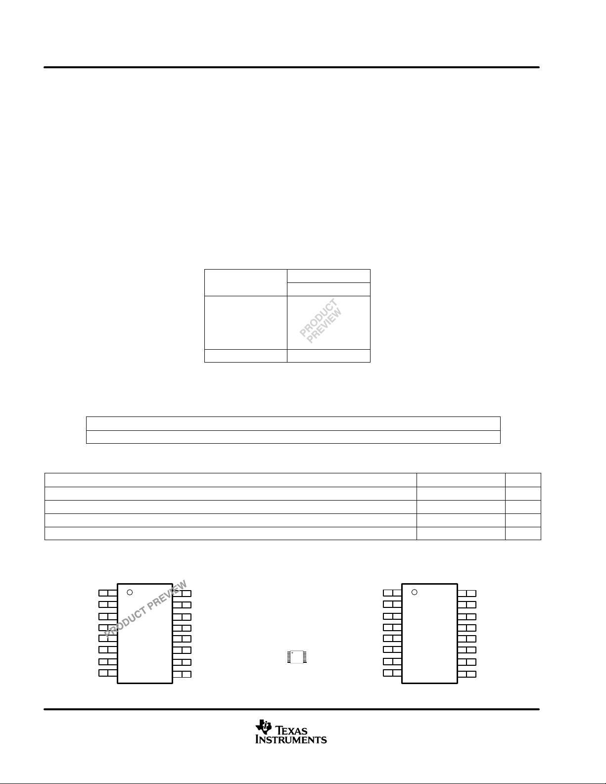
D TSSOP-16 (PW) Package
APPLICATIONS
D
Portable PCs
D Desktop LCD Monitors
D Internet Appliances
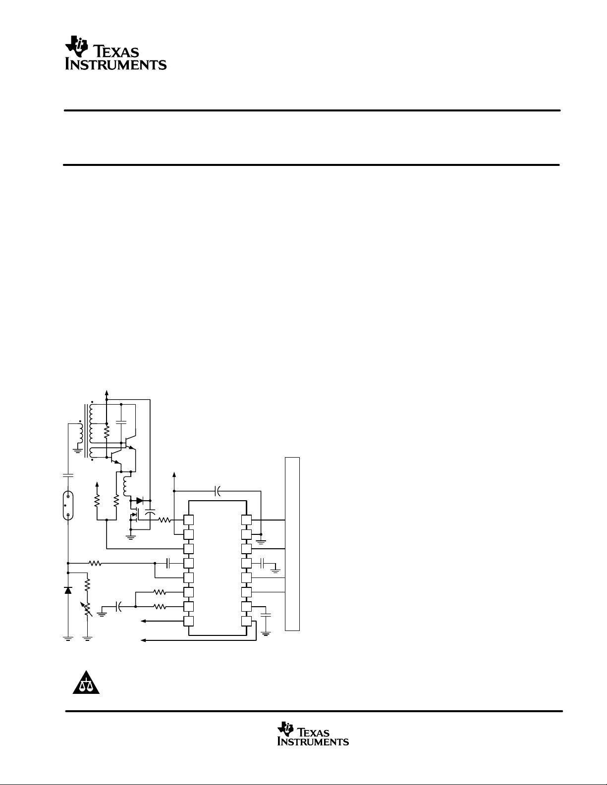
DESCRIPTION
Design goals for a cold cathode fluorescent lamp
(CCFL) converter used for a liquid crystal display
(LCD) monitor application include small size, high
efficiency, and low cost. The UCC2974/UCC3974
CCFL controllers provide the necessary circuit
blocks to implement a highly efficient LCD monitor
backlight supply in a small 16-pin TSSOP
package. The device features two control stages
for operating independent resonant tanks for
multi-lamp designs. The BiCMOS controller
typically consumes less than 2-mA of operating
current, improving overall system efficiency.
External parts count is minimized and system cost
is reduced by integrating such features as dual
PWM driver stages, open lamp protection,
overvoltage clamp, and synchronization circuitry
between the buck and push-pull stages. The
device operates in both analog and low-frequency
dimming modes.
Copyright 2001, Texas Instruments Incorporated
Please be aware that an important notice concerning availability, standard warranty, and use in critical applications of
Texas Instruments semiconductor products and disclaimers thereto appears at the end of this data sheet.
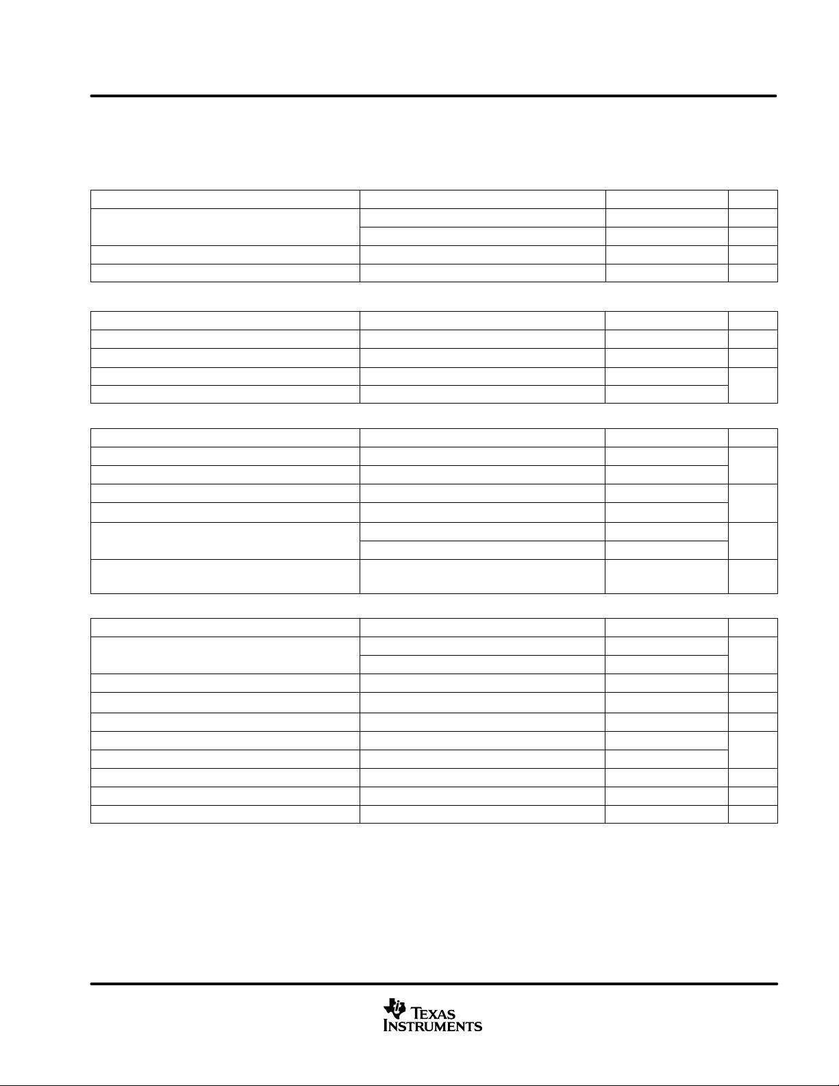
1 OUT1 16OUT2
2VIN 15GND
3 BUCK1 14BUCK2
4 COMP1 13CBP
5 FB1 12COMP2
6RC 11FB2
7RD 10MODE
8DIM 9LFDSYNC
UCC3974
VIN
VIN
VIN
BRIGHT
SYNC
MIRROR CHANNEL 1
TYPICAL APPLICATION
UDG–01023
SLUS485A – JULY 2001 – REVISED NOVEMBER 2001
2
www.ti.com
absolute maximum ratings over operating free-air temperature (unless otherwise noted)
†
Supply voltage range, VBAT 27 V. . . . . . . . . . . . . . . . . . . . . . . . . . . . . . . . . . . . . . . . . . . . . . . . . . . . . . . . . . . . . . . .
Input voltage range, BUCK –5 V to VBAT. . . . . . . . . . . . . . . . . . . . . . . . . . . . . . . . . . . . . . . . . . . . . . . . . . . . . . .
MODE –0.3 V to 4.3 V. . . . . . . . . . . . . . . . . . . . . . . . . . . . . . . . . . . . . . . . . . . . . . . . . . . . . .
Mode maximum forced current 300 µA. . . . . . . . . . . . . . . . . . . . . . . . . . . . . . . . . . . . . . . . . . . . . . . . . . . . . . . . . . . . .
Operating virtual junction temperature range, T
J
–55°C to 150°C. . . . . . . . . . . . . . . . . . . . . . . . . . . . . . . . . . . . . .
Storage temperature range, T
stg
–65°C to 150°C. . . . . . . . . . . . . . . . . . . . . . . . . . . . . . . . . . . . . . . . . . . . . . . . . . . .
Lead temperature soldering 1,6 mm (1/16 inch) from case for 10 seconds 260°C. . . . . . . . . . . . . . . . . . . . . . .
†
Stresses beyond those listed under “absolute maximum ratings” may cause permanent damage to the device. These are stress ratings only, and
functional operation of the device at these or any other conditions beyond those indicated under “recommended operating conditions” is not
implied. Exposure to absolute-maximum-rated conditions for extended periods may affect device reliability.
‡
Unless otherwise specified, all voltages are with respect to GND.
AVAILABLE OPTIONS
T
PACKAGE
T
J
PW
§
(SSOP)
–40_C to 85_C
UCC2974PW
0_C to 70_C UCC3974PW
§
This package is available taped and reeled. To
order this packaging option, add an R suffix to
the part number. (e.g. UCC2974PWR)
DISSIPATION RATING TABLE
PACKAGE
T
A
≤ 25°C DERATING FACTOR T
A
= 70°C T
A
= 85°C
16-pin PW with solder 775 mW 6.2 mW/°C 495 mW 402 mW
recommended operating conditions
MIN NOM MAX UNIT
Supply voltage, V
IN
4.5 25 V
Mode voltage 0 4.3 V
DIM voltage 0 3.5 V
LFDSYNC amplitude 0 4.5 V
1
2
3
4
5
6
7
8
16
15
14
13
12
11
10
9
OUT1
VIN
BUCK1
COMP1
FB1
RC
RD
DIM
OUT2
GND
BUCK2
CBP
COMP2
FB2
MODE
LFDSYNC
UCC2974
PW PACKAGE
(TOP VIEW)
ACTUAL SIZE
(5,10mm x 6,60mm)
1
2
3
4
5
6
7
8
16
15
14
13
12
11
10
9
OUT1
VIN
BUCK1
COMP1
FB1
RC
RD
DIM
OUT2
GND
BUCK2
CBP
COMP2
FB2
MODE
LFDSYNC
UCC3974
PW PACKAGE
(TOP VIEW)
SLUS485A – JULY 2001 – REVISED NOVEMBER 2001
3
www.ti.com
electrical characteristics over recommended operating virtual junction temperature range,
T
A
= 0_C to 70_C for the UCC3974, T
A
= –40_C to 85_C, for the UCC2974, T
A
= T
J.
V
IN
= V
BUCK
= 12 V, MODE = OPEN (unless otherwise noted)
supply current
PARAMETER TEST CONDITIONS MIN TYP MAX UNIT
I
V s ppl c rrent
12 V ≤ V
IN
≤ 25 V 1.7 3 mA
I
IN
V
IN
supply current
V
IN
= 12 V,
MODE < 0.425 V 300 500 µA
UVLO threshold voltage LOW to HIGH 3.6 4 4.4 V
UVLO hysteresis voltage 35 120 200 mV
output
PARAMETER TEST CONDITIONS MIN TYP MAX UNIT
High-level output voltage 12 V ≤ V
IN
≤ 25 V 8 10.5 13 V
Low-level output voltage MODE = 0.5 V, I
SINK
= 1 mA 50 200 mV
Rise time C
L
= 1 nF 170 350
ns
Fall time C
L
= 1 nF 140 300
ns
oscillator
PARAMETER TEST CONDITIONS MIN TYP MAX UNIT
Free-running oscillator frequency 12 V ≤ V
IN
≤ 25 V, BUCK = V
IN
30 45 60
kH
Free-running synchronizable oscillator frequency 12 V ≤ V
IN
≤ 25 V, BUCK = V
IN
–3 62 220
kHz
Maximum duty cycle FB = 1 V 100%
Minimum duty cycle FB = 2 V 0%
BUCK input bias current
BUCK = VIN = 12 V 3 10
A
BUCK input bias current
BUCK = VIN = 25 V 3 10
µA
Zero detect threshold voltage
Measured at BUCK with respect to V
IN
,
12 V ≤ V
IN
≤ 25 V
–2.4 –1.7 –1.1 V
error amplifier
PARAMETER TEST CONDITIONS MIN TYP MAX UNIT
Input voltage
COMP = FB, 0_C ≤ T
A
≤ 70_C 1.465 1.5 1.535
V
Input voltage
COMP = FB, –40_C ≤ T
A
≤ 85_C 1.455 1.5 1.545
V
Line regulation voltage 12 V ≤ V
IN
≤ 25 V 1 5 mV
Input bias current 100 250 nA
Open loop gain 60 80 dB
High-level output voltage FB = 1 V, I
SOURCE
= 50 µA 3.5 3.7 4.2
V
Low-level output voltage FB = 2 V, I
SINK
= 50 µA 0.15 0.35
V
Output source current FB = 1 V, COMP = 2 V –1.2 –0.3 mA
Output sink current FB = 2 V, COMP = 2 V 45 90 µA
Unity gain bandwidth T
J
= 25C, See Note 1 2 5 MHz
NOTE 1: Ensured by design, not production tested.
剩余13页未读,继续阅读
资源评论
不觉明了
- 粉丝: 3164
- 资源: 5429
上传资源 快速赚钱
- 我的内容管理 展开
- 我的资源 快来上传第一个资源
- 我的收益 登录查看自己的收益
- 我的积分 登录查看自己的积分
- 我的C币 登录后查看C币余额
- 我的收藏
- 我的下载
- 下载帮助
安全验证
文档复制为VIP权益,开通VIP直接复制
信息提交成功