TI-OPA2391.pdf
需积分: 10 97 浏览量
2022-11-22
23:33:21
上传
评论 5
收藏 2.5MB PDF 举报

OPAx391 Precision, Ultra-Low I
Q
, Low Offset Voltage, e-trim™ Operational Amplifiers
1 Features
• Low I
Q
: 24 µA
• Gain bandwidth product: 1 MHz
• Low input bias current: 10 fA
• Low offset voltage: ±45 µV (maximum)
• Low drift: ±1.2 µV/°C
• Low supply voltage operation: 1.7 V to 5.5 V
• Input common mode range ±100 mV beyond rail
• Fast slew rate: 1 V/µs
• High load capacitance drive
• High output current drive: 60 mA
• Rail-to-rail output
• EMI/RFI filtered inputs
• Small package options: SC-70, DSBGA
2 Applications
• Portable electronics
• Flow transmitter
• Blood glucose monitor
• Process analytics (pH, gas, force, humidity)
• Temperature transmitter
• Pressure transmitter
• Medical sensor patches
• Building automation
• Wearable fitness and activity monitor
• Gas detector
• Analog security camera
3 Description
The OPA391 and OPA2391 (OPAx391) feature a
unique combination of high bandwidth (1 MHz)
along with very-low quiescent current (24 µA) in
high-precision amplifiers. These features combined
with rail-to-rail input and output make these devices
an exceptional choice in high-gain, low-power
applications. Ultra-low input bias current of 10 fA,
only 45 µV of offset (maximum), and 1.2 µV/°C of
drift over temperature help maintain high precision in
ratiometric and amperometric sensor front ends that
have demanding low-power requirements.
The OPAx391 use Texas Instrument's proprietary
e‑trim
™
operational amplifier technology, enabling a
unique combination of ultra-low offset and low input
offset drift without the need for any input switching or
auto-zero techniques. The CMOS-based technology
platform also features a modern, robust output stage
design that is tolerant of high output capacitance,
alleviating stability problems that are common in
typical low-power amplifiers.
Device Information
PART NUMBER CHANNELS PACKAGE
(1)
OPA391
Single DCK (SC70, 5)
Single DBV (SOT-23, 5)
(3)
OPA2391
(2)
Dual D (SOIC, 8)
(3)
Dual DGK (VSSOP, 8)
(3)
Dual YBJ (DSBGA, 9)
(2)
OPA4391
(3)
Quad PW (TSSOP, 14)
(3)
(1) For all available packages, see the package option
addendum at the end of the data sheet.
(2) Preview with samples (not production data).
(3) Preview, no samples (not production data).
+
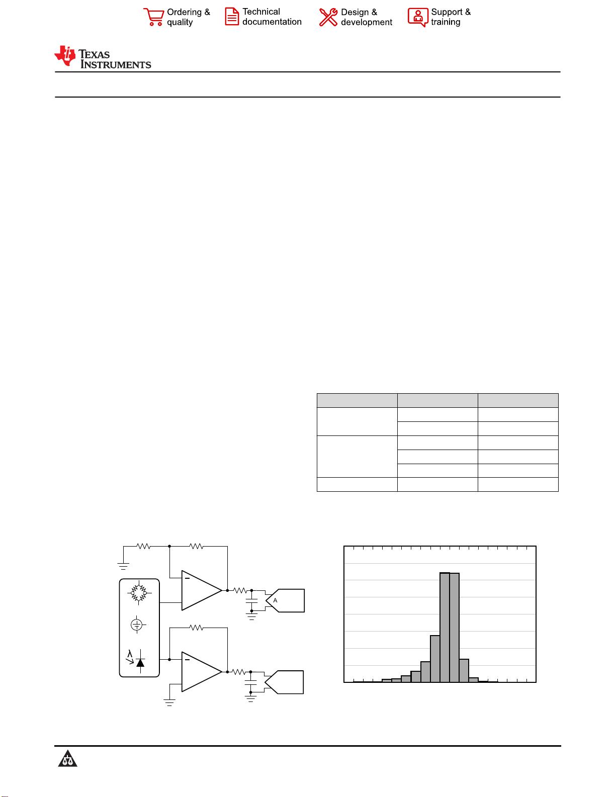
OPAx391
Sensors
Bridges
Transducers
Electrochemical Cells
Photodiodes
+
OPAx391
CE
RE
WE
ADS7042
ADS7042
High Input Impedance, Low Offset Buffer
Input Offset Voltage (PV)
Amplifiers (%)
-50 -40 -30 -20 -10 0 10 20 30 40 50
0
5
10
15
20
25
30
35
40
opa3
OPA391 Offset Voltage
OPA391, OPA2391
SBOS925B – DECEMBER 2020 – REVISED NOVEMBER 2022
An IMPORTANT NOTICE at the end of this data sheet addresses availability, warranty, changes, use in safety-critical applications,
intellectual property matters and other important disclaimers. UNLESS OTHERWISE NOTED, this document contains PRODUCTION
DATA.

剩余35页未读,继续阅读
资源评论


