没有合适的资源?快使用搜索试试~ 我知道了~
TI-ADC32RF54.pdf
需积分: 9 0 下载量 122 浏览量
2022-11-27
16:19:07
上传
评论 4
收藏 5.06MB PDF 举报
温馨提示
试读
104页
TI-ADC32RF54.pdf
资源推荐
资源详情
资源评论
ADC32RF5x Dual Channel 14-bit 2.6 to 3-GSPS RF Sampling Data Converter
1 Features
• 14-Bit, dual channel 2.6/3.0-GSPS ADC
• Noise spectral density:
– NSD = -156 dBFS/Hz (no AVG, 3 GSPS)
– NSD = -159 dBFS/Hz (2x AVG , 3 GSPS)
– NSD = -161 dBFS/Hz (4x AVG, 2.6 GSPS)
• Single core (non-interleaved) ADC architecture
• Aperture jitter: 50 fs
• Low close-in residual phase noise:
– -127 dBc/Hz at 10 kHz offset
• Spectral performance (f
IN
= 1 GHz, -1 dBFS):
– 2x internal averaging
– SNR: 64.7 dBFS
– SFDR HD2,3: 75 dBc
– SFDR worst spur: 90 dBFS
• Spectral performance (f
IN
= 1.8 GHz, -1 dBFS):
– 2x internal averaging
– SNR: 61.6 dBFS
– SFDR HD2,3: 70 dBc
– SFDR worst spur: 90 dBFS
• Input fullscale: 1.1/1.35 Vpp (2/3.5 dBm)
• Code error rate (CER): 10
-15
• Full power input bandwidth (-3 dB): 2.3 GHz
• JESD204B serial data interface
– Maximum lane rate: 13 Gbps
– Supports subclass 1 deterministic latency
• Digital down-converters
– Up to four DDC per ADC channel
– Complex output: 4x to 128x decimation
– 48-bit NCO phase coherent frequency hopping
– Fast frequency hopping: < 1 us
• Power consumption: 2.2 W/channel (2x AVG)
• Power supplies: 1.8 V, 1.2 V
2 Applications
• Phased array radar
• Spectrum analyzer
• Software defined radio (SDR)
• Electronic warfare
• High-speed digitizer
• Cable infrastructure
• Communications infrastructure
3 Description
The ADC32RF5x is a single core 14-bit, 2.6
GSPS to 3 GSPS, dual channel analog to digital
converters (ADC) that supports RF sampling with
input frequencies up to 4 GHz. The design maximizes
signal-to-noise ratio (SNR) and delivers a noise
spectral density of -156 dBFS/Hz. Using additional
internal ADCs along with on-chip signal averaging, the
noise density improves to -161 dBFS/Hz.
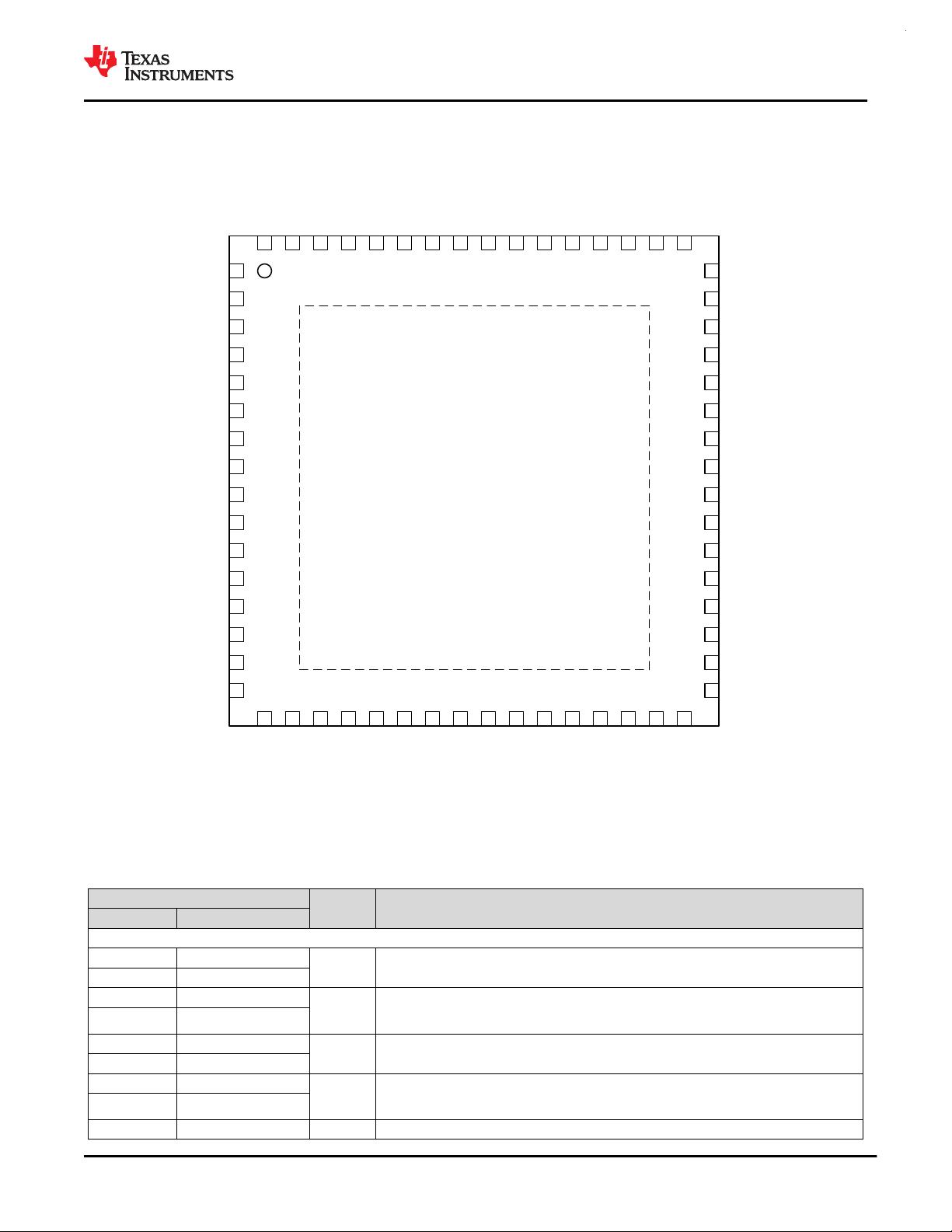
Each ADC channel can be connected to a quad-band
digital down-converter (DDC) using a 48-bit NCO
which supports phase coherent frequency hopping.
Using the GPIO pins for NCO frequency control,
frequency hopping can be achieved in less than 1 µs.
The ADC32RF54 and ADC32RF55 supports the
JESD204B serial data interface with subclass 1
deterministic latency using data rates up to 13 Gbps.
The power efficient ADC architecture consumes 1.8
W/ch at 3 Gsps and provides power scaling with lower
sampling rates.
Package Information
PART NUMBER PACKAGE
(1)
BODY SIZE (NOM)
ADC32RF5x QFN (64) 9.00 mm x 9.00 mm
(1) For all available packages, see the package option
addendum at the end of the data sheet.
Table 3-1. Device Comparison
PART NUMBER SAMPLING RATE
ADC32RF55 3.0 GSPS
ADC32RF54 2.6 GSPS
N
N
DDC
NCO
N
N
DDC
NCO
N
N
DDC
NCO
INA1P/M
SYSREFP/M
CLKP/M
100
3Gsps
ADC
DOUT0P/M
ADC
100
3Gsps
ADC
ADC
100
3Gsps
ADC
ADC
INB1P/M
100
3Gsps
ADC
ADC
N
N
DDC
NCO
1x/2x/4x Averaging
INA2P/M
INB2P/M
N
N
DDC
NCO
N
N
DDC
NCO
N
N
DDC
NCO
N
N
DDC
NCO
JESD204B
DOUT3P/M
DOUT4P/M
DOUT7P/M
1x/2x/4x Averaging
SEN
SCLK
SDIO
GPIO1
GPIO2
RESETb
SPISEL
SPI Registers and
Device Control
Block Diagram
ADVANCE INFORMATION
ADC32RF54
SBAS500 – JUNE 2022
An IMPORTANT NOTICE at the end of this data sheet addresses availability, warranty, changes, use in safety-critical applications,
intellectual property matters and other important disclaimers. ADVANCE INFORMATION for preproduction products; subject to change
without notice.
Table of Contents
1 Features............................................................................1
2 Applications..................................................................... 1
3 Description.......................................................................1
4 Revision History.............................................................. 2
5 Pin Configuration and Functions...................................3
6 Specifications.................................................................. 5
6.1 Absolute Maximum Ratings........................................ 5
6.2 ESD Ratings............................................................... 5
6.3 Recommended Operating Conditions.........................5
6.4 Thermal Information....................................................6
6.5 Electrical Characteristics - Power Consumption......... 7
6.6 Electrical Characteristics - DC Specifications............. 8
6.7 Electrical Characteristics - AC Specifications
(Dither DISABLED)........................................................9
6.8 Electrical Characteristics - AC Specifications
(Dither ENABLED).......................................................11
6.9 Timing Requirements................................................ 13
6.10 Typical Characteristics............................................15
7 Detailed Description......................................................27
7.1 Overview................................................................... 27
7.2 Functional Block Diagram......................................... 27
7.3 Feature Description...................................................28
7.4 Device Functional Modes..........................................57
7.5 Programming............................................................ 58
7.6 Register Maps...........................................................60
8 Application and Implementation.................................. 84
8.1 Application Information............................................. 84
8.2 Typical Applications.................................................. 84
8.3 Initialization Set Up................................................... 87
8.4 Power Supply Recommendations.............................94
8.5 Layout....................................................................... 96
9 Device and Documentation Support............................99
9.1 Receiving Notification of Documentation Updates....99
9.2 Support Resources................................................... 99
9.3 Trademarks............................................................... 99
9.4 Electrostatic Discharge Caution................................99
9.5 Glossary....................................................................99
10 Mechanical, Packaging, and Orderable
Information.................................................................... 99
4 Revision History
NOTE: Page numbers for previous revisions may differ from page numbers in the current version.
DATE REVISION NOTES
June 2022 * Initial Release
ADC32RF54
SBAS500 – JUNE 2022
www.ti.com
ADVANCE INFORMATION
2 Submit Document Feedback
Copyright © 2022 Texas Instruments Incorporated
Product Folder Links: ADC32RF54
5 Pin Configuration and Functions
1
2
3
4
5
6
7
8
9
10
11
12
13
14
15
16
17 18 19 20 21 22 23 24 25 26 27 28 29 30 31 32
48
47
46
45
44
43
42
41
40
39
38
37
36
35
34
33
64 63 62 61 60 59 58 57 56 55 54 53 52 51 50 49
DOUT1P
DOUT1M
DVDD
DOUT0P
DOUT0M
DGND
DVDD
DGND
DVDD
SPISEL
RESETb
AGND
AVDD12
INA1P
INA1M
AVDD12 AVDD12
DOUT5P
DOUT5M
DVDD
DOUT4P
DOUT4M
DGND
DVDD
DGND
DVDD
GPIO1
GPIO2
AGND
AVDD12
INB1P
INB1M
AVDD18
INA2P
INA2M
AVDD18
AVDD12
CLKGND
CLKP
CLKM
CLKVDD
VCM
SYSREFP
SYSREFM
AVDD18
INB2M
INB2P
AVDD18
GND PAD (backside)
DOUT6M
DOUT2M
DOUT2P
DGND
DOUT3M
DOUT3P
DVDD
AVDD18
SEN
SDIO
SCLK
DVDD
DOUT7P
DOUT7M
DGND
DOUT6P
Figure 5-1. RTD Package, 64 Pin VQFNP
(Top View)
Table 5-1. Pin Functions
PIN
TYPE
(1)
DESCRIPTION
NAME NO.
ANALOG INPUTS
INA1P 14
I Differential analog input for channel A. 100 Ω (default) or 50 Ω differential internal termination.
INA1M 15
INA2P 18
I
Differential analog input for alternate channel A input. This input is used for additional ADC
averaging for channel A. 100 Ω (default) or 50 Ω differential internal termination. Should be
connected to GND if unused.
INA2M 19
INB1P 35
I Differential analog input for channel B. 100 Ω (default) or 50 Ω differential internal termination.
INB1M 34
INB2P 31
I
Differential analog input for alternate channel B input. This input is used for additional ADC
averaging for channel B. 100 Ω (default) or 50 Ω differential internal termination. Should be
connected to GND if unused.
INB2M 30
VCM 26 O Common-mode voltage output for the analog inputs.
www.ti.com
ADC32RF54
SBAS500 – JUNE 2022
ADVANCE INFORMATION
Copyright © 2022 Texas Instruments Incorporated
Submit Document Feedback
3
Product Folder Links: ADC32RF54
Table 5-1. Pin Functions (continued)
PIN
TYPE
(1)
DESCRIPTION
NAME NO.
CLOCK, SYNCHRONIZATION
CLKP 23
I Differential sampling clock input. 100 Ω differential internal termination.
CLKM 24
SYSREFP 27
I Differential external synchronization input.
SYSREFM 28
CONTROL
RESETb 11 I Hardware reset. Active low. This pin has an internal 21 kΩ pullup resistor to AVDD18.
SEN 57 I Serial interface enable. Active low. This pin has an internal 21 kΩ pull-up resistor to AVDD18.
SCLK 55 I Serial interface clock input. This pin has an internal 21 kΩ pull-down resistor.
SDIO 56 I/O Serial interface data input and output. This pin has an internal 21 kΩ pull-down resistor.
GPIO1 39 I
GPIO control pin. This pin is configured through SPI interface for power down or NCO control
function.
GPIO2 38 I
GPIO control pin. This pin is configured through SPI interface for power down or NCO control
function.
SPISEL 10 I
Determines SPI control: either normal SPI for register writes or fast access to NCO selection only
for fast frequency hopping.
DIGITAL DATA INTERFACE
DOUT0P 4
O JESD204B high-speed serial data output interface pins for channel A.
DOUT0M 5
DOUT1P 1
DOUT1M 2
DOUT2P 63
DOUT2M 64
DOUT3P 60
DOUT3M 61
DOUT4P 45
O JESD204B high-speed serial data output interface pins for channel B.
DOUT4M 44
DOUT5P 48
DOUT5M 47
DOUT6P 50
DOUT6M 49
DOUT7P 53
DOUT7M 52
POWER SUPPLY
AVDD18 17,20,29,32, 58 I Analog 1.8-V power supply
AVDD12 13,16,21,33, 36 I Analog 1.2-V power supply
CLKVDD 25 I
Clock 1.2-V power supply. Very sensitive to power supply noise. Directly impacts close in aperture
phase noise.
DVDD 3,7,9,40,42, 46,54,59 I Digital 1.2-V power supply
AGND 12,37 I Analog ground, shorted to thermal pad.
CLKGND 22 I Clock ground.
DGND 6,8,41,43,51,62 I Digital ground.
(1) I = Input, O = Output, I/O = Input or Output.
ADC32RF54
SBAS500 – JUNE 2022
www.ti.com
ADVANCE INFORMATION
4 Submit Document Feedback
Copyright © 2022 Texas Instruments Incorporated
Product Folder Links: ADC32RF54
6 Specifications
6.1 Absolute Maximum Ratings
over operating free-air temperature range (unless otherwise noted)
(1)
PARAMETER TEST CONDITIONS MIN MAX UNIT
Supply voltage range, AVDD18 –0.3 2.1 V
Supply voltage range, AVDD12/CLKVDD/DVDD –0.3 1.4 V
Voltage applied to input pins
INA1P/M, INB1P/M, INA2P/M, INB2P/M –0.6 1.2
V
CLKP/M –0.3 VDDCLK + 0.3
SYSREFP/M –0.3 AVDD12 + 0.6
GPIO1/2, PDN, RESET, SCLK, SEN, SDIO, SPISEL –0.3 AVDD18 + 0.2
Peak RF input power (INx1P/M, INx2P/M) Differential 100 Ω termination. 12 dBm
Junction temperature, T
J
115 °C
Storage temperature, T
stg
–65 150 °C
(1) Stresses beyond those listed under Absolute Maximum Ratings may cause permanent damage to the device. These are stress
ratings only, which do not imply functional operation of the device at these or any other conditions beyond those indicated under
Recommended Operating Conditions. Exposure to absolute-maximum-rated conditions for extended periods may affect device
reliability.
6.2 ESD Ratings
VALUE UNIT
V
(ESD)
Electrostatic
discharge
Human body model (HBM), per ANSI/ESDA/JEDEC JS-001
(1)
± 1000
V
Charged device model (CDM), per ANSI/ESDA/JEDEC JS-002
(2)
± 500
(1) JEDEC document JEP155 states that 500-V HBM allows safe manufacturing with a standard ESD control process.
(2) JEDEC document JEP157 states that 250-V CDM allows safe manufacturing with a standard ESD control process.
6.3 Recommended Operating Conditions
over operating free-air temperature range (unless otherwise noted)
MIN NOM MAX UNIT
AVDD18 1.8 V analog supply 1.75 1.8 1.85
V
AVDD12 1.2 V analog supply 1.175 1.2 1.225
CLKVDD 1.2 V clock supply 1.175 1.2 1.225
DVDD 1.2 V digital supply 1.175 1.2 1.225
T
A
Operating free-air temperature –40 85 °C
T
J
Operating junction temperature 105
(1)
°C
(1) Prolonged use above this junction temperature may increase the device failure-in-time (FIT) rate.
www.ti.com
ADC32RF54
SBAS500 – JUNE 2022
ADVANCE INFORMATION
Copyright © 2022 Texas Instruments Incorporated
Submit Document Feedback
5
Product Folder Links: ADC32RF54
剩余103页未读,继续阅读
资源评论
不觉明了
- 粉丝: 3119
- 资源: 5348
上传资源 快速赚钱
- 我的内容管理 展开
- 我的资源 快来上传第一个资源
- 我的收益 登录查看自己的收益
- 我的积分 登录查看自己的积分
- 我的C币 登录后查看C币余额
- 我的收藏
- 我的下载
- 下载帮助
安全验证
文档复制为VIP权益,开通VIP直接复制
信息提交成功