没有合适的资源?快使用搜索试试~ 我知道了~
TI-ADC08DJ5200RF.pdf TI-ADC08DJ5200RF 是一款单通道或双通道、8 位、RF 采样模拟数字转换器(ADC),其主要特点包括: * 高速采样率:单通道模式下最高可达 10.4 GSPS,双通道模式下最高可达 5.2 GSPS * 低噪声特性:双通道模式下噪声.floor 为 -143.4 dBFS/Hz,单通道模式下为 -146.2 dBFS/Hz * 高带宽输入:模拟输入带宽达 8.1 GHz,usable input frequency range 高达 10 GHz * 静态延迟调整:具有精确的采样控制,步长为 19 fs,简化了同步和交错操作 * 易于使用的同步功能:自动 SYSREF 定时器校准、时间戳标记 * JESD204C 串行数据接口:最高 lane 速率为 17.16 Gbps,支持 64b/66b 和 8b/10b 编码 * 高峰 RF 输入功率:+26.5 dBm (+27.5 dBFS,560 倍 fullscale 功率) * 可编程的 FIR 滤波器用于均衡 * 低功耗:仅 3.8 W * 双电源供电:1.1 V 和 1.9 V 该设备广泛应用于: * 示波器和宽带数字化器 * 通信测试器(802.11ad、5G) * 电子战(SIGINT、ELINT) * 卫星通信(SATCOM) * RF 采样软件定义无线电(SDR) * 光谱仪 ADC08DJ5200RF 的高采样率和低噪声特性使其成为 RF 采样应用的不二之选。同时,该设备还支持多种应用场景,例如电子战、卫星通信、RF 采样软件定义无线电等。
资源推荐
资源详情
资源评论

ADC08DJ5200RF 10.4-GSPS Single-Channel or 5.2-GSPS Dual-Channel, 8-bit, RF-
Sampling Analog-to-Digital Converter (ADC)
1 Features
• ADC core:
– 8-bit resolution
– Up to 10.4 GSPS in single-channel mode
– Up to 5.2 GSPS in dual-channel mode
• Performance specifications:
– Noise floor (–20 dBFS, V
FS
= 1 V
PP-DIFF
):
• Dual-channel mode: –143.4 dBFS/Hz
• Single-channel mode: –146.2 dBFS/Hz
– ENOB (dual channel, F
IN
= 2.4 GHz, TYP): 7.8
Bits
• Buffered analog inputs with V
CMI
of 0 V:
– Analog input bandwidth (–3 dB): 8.1 GHz
– Usable input frequency range: > 10 GHz
– Full-scale input voltage (V
FS
, default): 0.8 V
PP
• Noiseless aperture delay (t
AD
) adjustment:
– Precise sampling control: 19-fs Step
– Simplifies synchronization and interleaving
– Temperature and voltage invariant delays
• Easy-to-use synchronization features:
– Automatic SYSREF timing calibration
– Timestamp for sample marking
• JESD204C serial data interface:
– Maximum lane rate: 17.16 Gbps
– Support for 64b/66b and 8b/10b encoding
– 8b/10b modes are JESD204B compatible
• Peak RF Input Power (Diff): +26.5 dBm (+ 27.5
dBFS, 560x fullscale power)
• Programmable FIR filter for equalization
• Power consumption: 3.8 W
• Power supplies: 1.1 V, 1.9 V
2 Applications
• Oscilloscopes and wideband digitizers
• Communications testers (802.11ad, 5G)
• Electronic warfare (SIGINT, ELINT)
• Satellite communications (SATCOM)
• RF-sampling software-defined radio (SDR)
• Spectrometry
3 Description
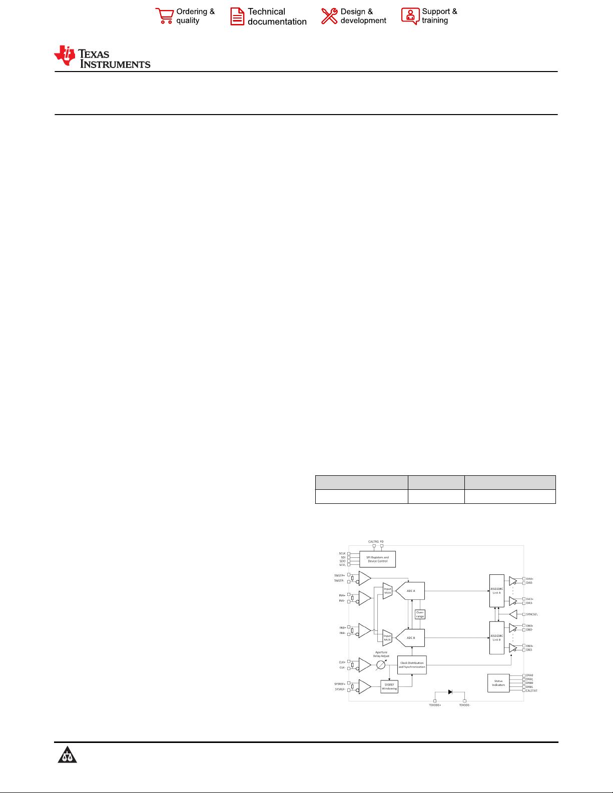
The ADC08DJ5200RF device is an RF-sampling,
giga-sample, analog-to-digital converter (ADC) that
directly samples input frequencies from DC to above
10 GHz. The ADC08DJ5200RF can be configured as
a dual-channel, 5.2 GSPS ADC or single-channel,
10.4 GSPS ADC. Support of a useable input
frequency range of up to 10 GHz enables direct RF
sampling of L-band, S-band, C-band, and X-band for
frequency agile systems.
The ADC08DJ5200RF uses a high-speed JESD204C
output interface with up to 16 serialized lanes
supporting up to 17.16 Gbps line rate. Deterministic
latency and multi-device synchronization is supported
through JESD204C subclass-1. The JESD204C
interface can be configured to trade-off line rate and
number of lanes. Both 8b/10b and 64b/66b data
encoding schemes are supported. 64b/66b encoding
supports forward error correction (FEC) for improved
bit error rates. The interface is backwards compatible
with JESD204B receivers.
Innovative synchronization features, including
noiseless aperture delay adjustment and SYSREF
windowing, simplify system design for multi-channel
applications. A programmable FIR filter allows on-chip
equalization.
Device Information
PART NUMBER PACKAGE
(1)
BODY SIZE (NOM)
ADC08DJ5200RF FCBGA (144) 10.00 mm × 10.00 mm
(1) For all available packages, see the package option
addendum at the end of the data sheet.
ADC08DJ5200RF Block Diagram
ADC08DJ5200RF
SLVSEO1 – AUGUST 2021
An IMPORTANT NOTICE at the end of this data sheet addresses availability, warranty, changes, use in safety-critical applications,
intellectual property matters and other important disclaimers. PRODUCTION DATA.

Table of Contents
1 Features............................................................................1
2 Applications..................................................................... 1
3 Description.......................................................................1
4 Revision History.............................................................. 2
5 Pin Configuration and Functions...................................3
6 Specifications.................................................................. 8
6.1 Absolute Maximum Ratings ....................................... 8
6.2 ESD Ratings .............................................................. 8
6.3 Recommended Operating Conditions ........................9
6.4 Thermal Information ...................................................9
6.5 Electrical Characteristics: DC Specifications ........... 10
6.6 Electrical Characteristics: Power Consumption ....... 12
6.7 Electrical Characteristics: AC Specifications
(Dual-Channel Mode) ................................................. 13
6.8 Electrical Characteristics: AC Specifications
(Single-Channel Mode) .............................................. 18
6.9 Timing Requirements ...............................................24
6.10 Switching Characteristics .......................................25
6.11 Typical Characteristics............................................ 28
7 Detailed Description......................................................49
7.1 Overview................................................................... 49
7.2 Functional Block Diagram......................................... 50
7.3 Feature Description...................................................51
7.4 Device Functional Modes..........................................73
7.5 Programming............................................................ 87
7.6 SPI Register Map......................................................89
8 Application Information Disclaimer........................... 143
8.1 Application Information........................................... 143
8.2 Typical Applications................................................ 143
8.3 Initialization Set Up................................................. 145
9 Power Supply Recommendations..............................146
9.1 Power Sequencing..................................................147
10 Layout.........................................................................148
10.1 Layout Guidelines................................................. 148
10.2 Layout Example.................................................... 149
11 Device and Documentation Support........................152
11.1 Device Support......................................................152
11.2 Documentation Support........................................ 152
11.3 Receiving Notification of Documentation Updates 153
11.4 Support Resources............................................... 153
11.5 Trademarks........................................................... 153
11.6 Electrostatic Discharge Caution............................ 153
11.7 Glossary................................................................ 153
4 Revision History
NOTE: Page numbers for previous revisions may differ from page numbers in the current version.
DATE REVISION NOTES
August 2021 * Initial release.
ADC08DJ5200RF
SLVSEO1 – AUGUST 2021
www.ti.com
2 Submit Document Feedback
Copyright © 2021 Texas Instruments Incorporated
Product Folder Links: ADC08DJ5200RF

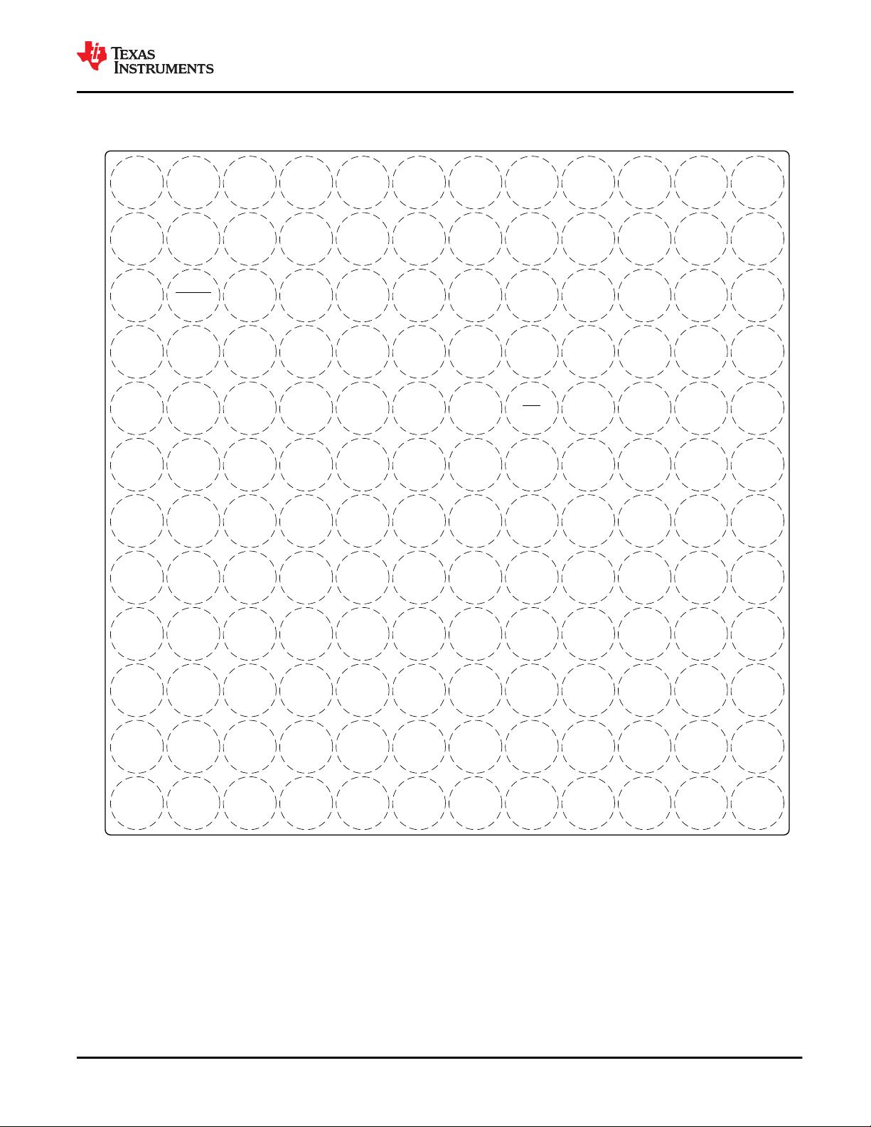
5 Pin Configuration and Functions
1 2 3 4 5 6 7 8 9 10 11 12
A
B
C
D
E
F
G
H
J
K
L
M
Not to scale
AGND AGND AGND INA+ INA± AGND AGND DA3+ DA3± DA2+ DA2± DGND
TMSTP+ AGND AGND AGND AGND AGND AGND DA7+ DA7± DA6+ DA6± DGND
TMSTP± SYNCSE BG VA19 VA11 AGND NCOA0 ORA0 VD11 VD11 DA5+ DA1+
AGND VA11 VA11 VA19 VA11 AGND NCOA1 ORA1 DGND DGND DA5± DA1±
AGND VA19 VA19 VA19 VA11 AGND CALTRIG SCS VD11 VD11 DA4+ DA0+
CLK+ AGND AGND VA19 VA11 AGND CALSTAT SCLK DGND DGND DA4± DA0±
CLK± AGND AGND VA19 VA11 AGND VD11 SDI DGND DGND DB4± DB0±
AGND VA19 VA19 VA19 VA11 AGND VD11 SDO VD11 VD11 DB4+ DB0+
AGND VA11 VA11 VA19 VA11 AGND NCOB1 ORB1 DGND DGND DB5± DB1±
SYSREF+ TDIODE+ TDIODE± VA19 VA11 PD NCOB0 ORB0 VD11 VD11 DB5+ DB1+
SYSREF± AGND AGND AGND AGND AGND AGND DB7+ DB7± DB6+ DB6± DGND
AGND AGND AGND INB+ INB± AGND AGND DB3+ DB3± DB2+ DB2± DGND
Figure 5-1. AAV Package, 144-Ball Flip Chip BGA, Top View
www.ti.com
ADC08DJ5200RF
SLVSEO1 – AUGUST 2021
Copyright © 2021 Texas Instruments Incorporated
Submit Document Feedback
3
Product Folder Links: ADC08DJ5200RF

Table 5-1. Pin Functions
PIN
I/O DESCRIPTION
NAME NO.
AGND
A1, A2, A3,
A6, A7, B2,
B3, B4, B5,
B6, B7, C6,
D1, D6, E1,
E6, F2, F3, F6,
G2, G3, G6,
H1, H6, J1, J6,
L2, L3, L4, L5,
L6, L7, M1,
M2, M3, M6,
M7
—
Analog supply ground. Tie AGND and DGND to a common ground plane (GND) on the circuit
board.
BG C3 O
Band-gap voltage output. This pin is capable of sourcing only small currents and driving limited
capacitive loads, as specified in the Recommended Operating Conditions table. This pin can be
left disconnected if not used.
CALSTAT F7 O
Foreground calibration status output or device alarm output. Functionality is programmed through
CAL_STATUS_SEL. This pin can be left disconnected if not used.
CALTRIG E7 I
Foreground calibration trigger input. This pin is only used if hardware calibration triggering is
selected in CAL_TRIG_EN, otherwise software triggering is performed using CAL_SOFT_TRIG.
Tie this pin to GND if not used.
CLK+ F1 I
Device (sampling) clock positive input. The clock signal is strongly recommended to be AC-
coupled to this input for best performance. In single-channel mode, the analog input signal is
sampled on both the rising and falling edges. In dual-channel mode, the analog signal is sampled
on the rising edge. This differential input has an internal untrimmed 100-Ω differential termination
and is self-biased to the optimal input common-mode voltage as long as DEVCLK_LVPECL_EN is
set to 0.
CLK– G1 I
Device (sampling) clock negative input. TI strongly recommends using AC-coupling for best
performance.
DA0+ E12 O
High-speed serialized data output for channel A, lane 0, positive connection. This differential
output must be AC-coupled and must always be terminated with a 100-Ω differential termination at
the receiver. This pin can be left disconnected if not used.
DA0– F12 O
High-speed serialized data output for channel A, lane 0, negative connection. This pin can be left
disconnected if not used.
DA1+ C12 O
High-speed serialized data output for channel A, lane 1, positive connection. This differential
output must be AC-coupled and must always be terminated with a 100-Ω differential termination at
the receiver. This pin can be left disconnected if not used.
DA1– D12 O
High-speed serialized data output for channel A, lane 1, negative connection. This pin can be left
disconnected if not used.
DA2+ A10 O
High-speed serialized-data output for channel A, lane 2, positive connection. This differential
output must be AC-coupled and must always be terminated with a 100-Ω differential termination at
the receiver. This pin can be left disconnected if not used.
DA2– A11 O
High-speed serialized-data output for channel A, lane 2, negative connection. This pin can be left
disconnected if not used.
DA3+ A8 O
High-speed serialized-data output for channel A, lane 3, positive connection. This differential
output must be AC-coupled and must always be terminated with a 100-Ω differential termination at
the receiver. This pin can be left disconnected if not used.
DA3– A9 O
High-speed serialized-data output for channel A, lane 3, negative connection. This pin can be left
disconnected if not used.
DA4+ E11 O
High-speed serialized data output for channel A, lane 4, positive connection. This differential
output must be AC-coupled and must always be terminated with a 100-Ω differential termination at
the receiver. This pin can be left disconnected if not used.
DA4– F11 O
High-speed serialized data output for channel A, lane 4, negative connection. This pin can be left
disconnected if not used.
DA5+ C11 O
High-speed serialized data output for channel A, lane 5, positive connection. This differential
output must be AC-coupled and must always be terminated with a 100-Ω differential termination at
the receiver. This pin can be left disconnected if not used.
ADC08DJ5200RF
SLVSEO1 – AUGUST 2021
www.ti.com
4 Submit Document Feedback
Copyright © 2021 Texas Instruments Incorporated
Product Folder Links: ADC08DJ5200RF

Table 5-1. Pin Functions (continued)
PIN
I/O DESCRIPTION
NAME NO.
DA5– D11 O
High-speed serialized data output for channel A, lane 5, negative connection. This pin can be left
disconnected if not used.
DA6+ B10 O
High-speed serialized data output for channel A, lane 6, positive connection. This differential
output must be AC-coupled and must always be terminated with a 100-Ω differential termination at
the receiver. This pin can be left disconnected if not used.
DA6– B11 O
High-speed serialized data output for channel A, lane 6, negative connection. This pin can be left
disconnected if not used.
DA7+ B8 O
High-speed serialized data output for channel A, lane 7, positive connection. This differential
output must be AC-coupled and must always be terminated with a 100-Ω differential termination at
the receiver. This pin can be left disconnected if not used.
DA7– B9 O
High-speed serialized data output for channel A, lane 7, negative connection. This pin can be left
disconnected if not used.
DB0+ H12 O
High-speed serialized data output for channel B, lane 0, positive connection. This differential
output must be AC-coupled and must always be terminated with a 100-Ω differential termination at
the receiver. This pin can be left disconnected if not used.
DB0– G12 O
High-speed serialized data output for channel B, lane 0, negative connection. This pin can be left
disconnected if not used.
DB1+ K12 O
High-speed serialized data output for channel B, lane 1, positive connection. This differential
output must be AC-coupled and must always be terminated with a 100-Ω differential termination at
the receiver. This pin can be left disconnected if not used.
DB1– J12 O
High-speed serialized data output for channel B, lane 1, negative connection. This pin can be left
disconnected if not used.
DB2+ M10 O
High-speed serialized data output for channel B, lane 2, positive connection. This differential
output must be AC-coupled and must always be terminated with a 100-Ω differential termination at
the receiver. This pin can be left disconnected if not used.
DB2– M11 O
High-speed serialized data output for channel B, lane 2, negative connection. This pin can be left
disconnected if not used.
DB3+ M8 O
High-speed serialized data output for channel B, lane 3, positive connection. This differential
output must be AC-coupled and must always be terminated with a 100-Ω differential termination at
the receiver. This pin can be left disconnected if not used.
DB3– M9 O
High-speed serialized data output for channel B, lane 3, negative connection. This pin can be left
disconnected if not used.
DB4+ H11 O
High-speed serialized data output for channel B, lane 4, positive connection. This differential
output must be AC-coupled and must always be terminated with a 100-Ω differential termination at
the receiver. This pin can be left disconnected if not used.
DB4– G11 O
High-speed serialized data output for channel B, lane 4, negative connection. This pin can be left
disconnected if not used.
DB5+ K11 O
High-speed serialized data output for channel B, lane 5, positive connection. This differential
output must be AC-coupled and must always be terminated with a 100-Ω differential termination at
the receiver. This pin can be left disconnected if not used.
DB5– J11 O
High-speed serialized data output for channel B, lane 5, negative connection. This pin can be left
disconnected if not used.
DB6+ L10 O
High-speed serialized data output for channel B, lane 6, positive connection. This differential
output must be AC-coupled and must always be terminated with a 100-Ω differential termination at
the receiver. This pin can be left disconnected if not used.
DB6– L11 O
High-speed serialized data output for channel B, lane 6, negative connection. This pin can be left
disconnected if not used.
DB7+ L8 O
High-speed serialized data output for channel B, lane 7, positive connection. This differential
output must be AC-coupled and must always be terminated with a 100-Ω differential termination at
the receiver. This pin can be left disconnected if not used.
DB7– L9 O
High-speed serialized data output for channel B, lane 7, negative connection. This pin can be left
disconnected if not used.
www.ti.com
ADC08DJ5200RF
SLVSEO1 – AUGUST 2021
Copyright © 2021 Texas Instruments Incorporated
Submit Document Feedback
5
Product Folder Links: ADC08DJ5200RF
剩余158页未读,继续阅读
资源评论

不觉明了
- 粉丝: 3992
- 资源: 5759
上传资源 快速赚钱
 我的内容管理
展开
 我的资源
快来上传第一个资源
 我的收益 登录查看自己的收益
 我的积分
登录查看自己的积分
 我的C币
登录后查看C币余额
 我的收藏
我的收藏  我的下载
我的下载  下载帮助
下载帮助

 前往需求广场,查看用户热搜
最新资源
- Untitled7.ipynb
- C#ASP.NET酒店管理系统源码 宾馆管理系统源码数据库 SQL2008源码类型 WebForm
- 【安卓毕业设计】基于安卓的奶牛管理源码(完整前后端+mysql+说明文档).zip
- 【安卓毕业设计】Android app作业源码(完整前后端+mysql+说明文档).zip
- Scrapy基础(讲解详细、包括框架流程代码实战,最佳学习资料).zip
- FPGA实现IIC通信quartus工程,纯verliog,可进行移植
- C#ASP.NET外贸订单管理系统源码 汽配订单管理系统源码数据库 SQL2008源码类型 WebForm
- 基于双流Faster R-CNN网络的图像篡改检测项目源码+训练好的模型+文档说明.zip
- 买的USB转485串口的驱动程序,使用的是美国TI芯片+WCH340芯片
- 二次平台培训视频,人事管理
资源上传下载、课程学习等过程中有任何疑问或建议,欢迎提出宝贵意见哦~我们会及时处理!
点击此处反馈


安全验证
文档复制为VIP权益,开通VIP直接复制
 信息提交成功