没有合适的资源?快使用搜索试试~ 我知道了~
TI-TLV320ADC6120.pdf
需积分: 5 0 下载量 160 浏览量
2022-12-03
19:42:30
上传
评论 4
收藏 5.35MB PDF 举报
温馨提示
试读
130页
TI-TLV320ADC6120.pdf
资源推荐
资源详情
资源评论
TLV320ADC6120 2-Channel, 768-kHz, Burr-Brown
TM
Audio ADC
1 Features
• Multichannel high-performance ADC:
– 2-channel analog microphones or line-in
– 4-channel digital PDM microphones
– Up to 2 analog and up to 2 digital microphone
channels
• ADC line and microphone differential input
performance:
– Dynamic range (DR):
• 123-dB, dynamic range enhancer (DRE)
enabled
• 113-dB, DRE disabled
– THD+N: –95 dB
• ADC channel summing mode, DR performance:
– 116-dB, DRE disabled, 2-channel summing
• ADC input voltage:
– Differential, 2-V
RMS
full-scale inputs
– Single-ended, 1-V
RMS
full-scale inputs
• ADC sample rate (f
S
) = 8 kHz to 768 kHz
• Programmable channel settings:
– Channel gain: 0 dB to 42 dB, 0.5-dB steps
– Digital volume control: –100 dB to 27 dB
– Gain calibration with 0.1-dB resolution
– Phase calibration with 163-ns resolution
• Programmable microphone bias or supply voltage
generation
• Low-latency signal processing filter selection
• Programmable HPF and biquad digital filters
• Automatic gain controller (AGC)
• Voice activity detection (VAD)
• I
2
C control interface
• Integrated high-performance audio PLL
• Automatic clock divider setting configurations
• Audio serial data interface:
– Format: TDM, I
2
S, or left-justified (LJ)
– Word length: 16 bits, 20 bits, 24 bits, or 32 bits
– Master or slave interface
• Single-supply operation: 3.3 V or 1.8 V
• I/O-supply operation: 3.3 V or 1.8 V
• Power consumption for 1.8-V AVDD supply:
– 9.5 mW/channel at 48-kHz sample rate
2 Applications
• Smart speakers
• IP network cameras
• Professional microphones and wireless systems
• Video conference systems
3 Description
The TLV320ADC6120 is a Burr-Brown
™
high-
performance, audio analog-to-digital converter (ADC)
that supports simultaneous sampling of up to two
analog channels or four digital channels for the
pulse density modulation (PDM) microphone input.
The device supports line and microphone inputs, and
allows for both single-ended and differential input
configurations. The device integrates programmable
channel gain, digital volume control, a programmable
microphone bias voltage, a phase-locked loop (PLL),
a programmable high-pass filter (HPF), biquad filters,
low-latency filter modes, and allows for sample
rates up to 768 kHz, and allows for sample rates
up to 192 kHz. The device supports time-division
multiplexing (TDM), I
2
S, or left-justified (LJ) audio
formats, and can be controlled with the I
2
C interface.
These integrated high-performance features, along
with the ability to be powered from a single-supply
of 3.3 V or 1.8 V, make the device an excellent
choice for space-constrained audio systems in far-
field microphone recording applications.
The TLV320ADC6120 is specified from –40°C to
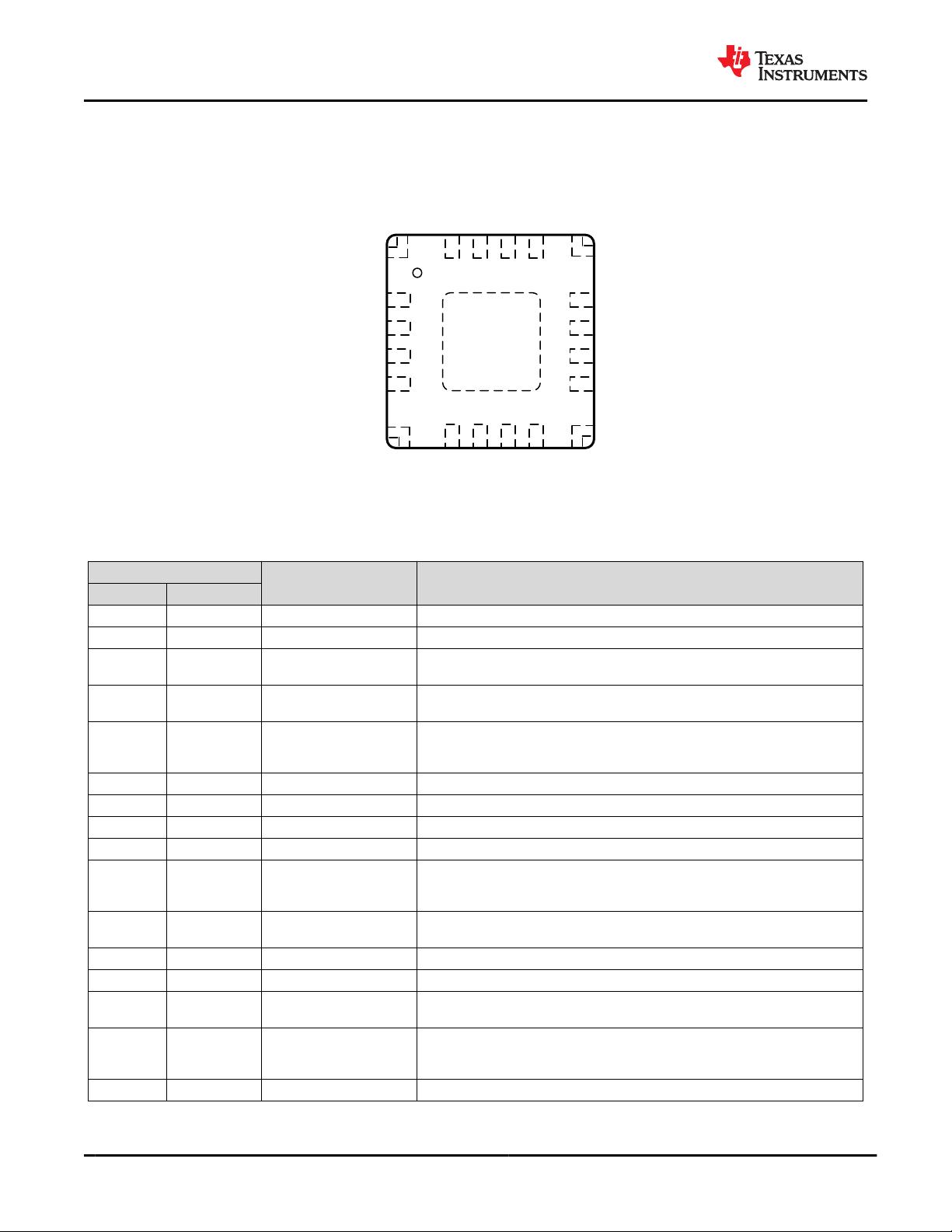
+125°C, and is offered in a 20-pin WQFN package.
Device Information
(1)
PART NUMBER PACKAGE BODY SIZE (NOM)
TLV320ADC6120 WQFN (20)
3.00 mm × 3.00 mm with
0.5-mm pitch
(1) For all available packages, see the package option
addendum at the end of the data sheet.
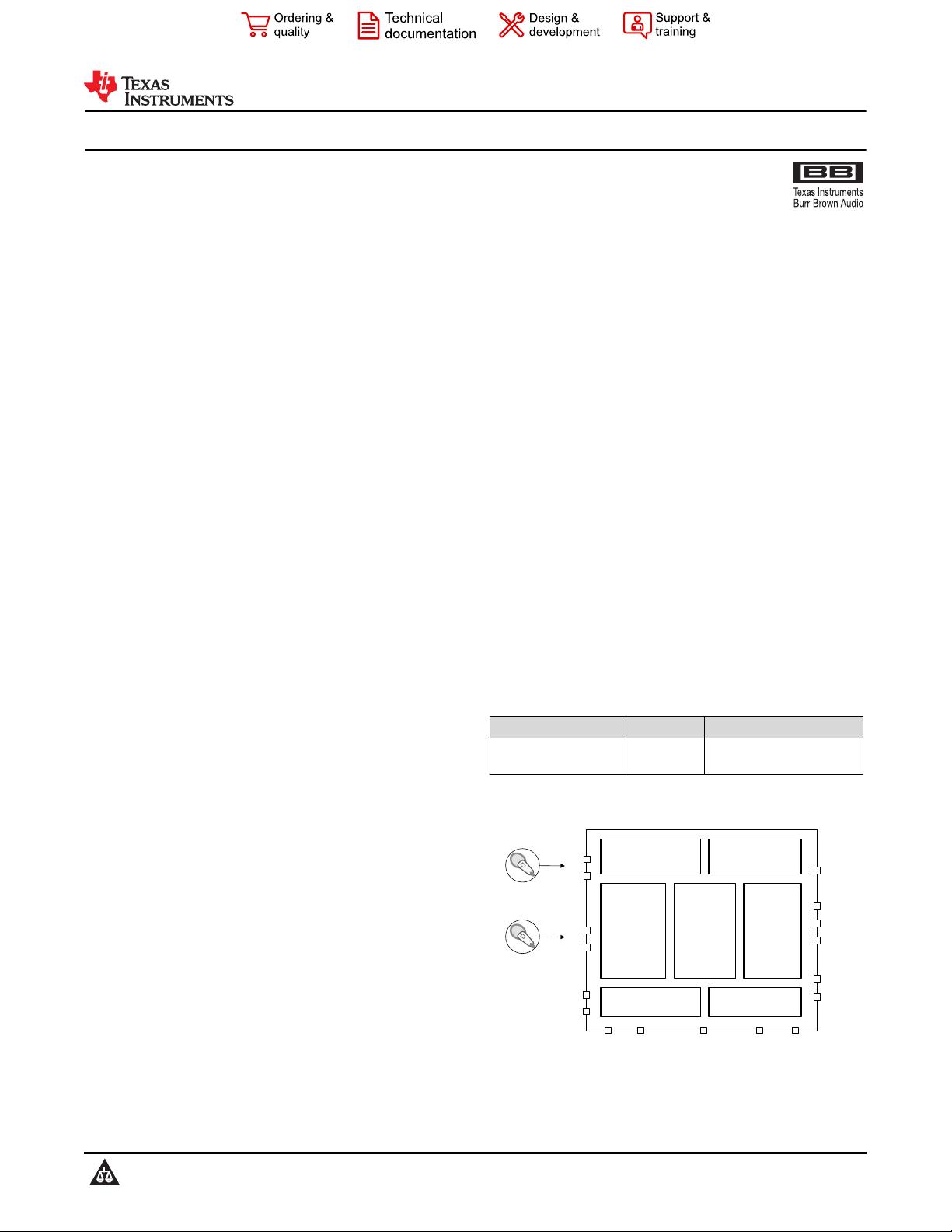
Audio Serial
Interface
(TDM, I
2
S, LJ)
PLL and Clock
Generation
Digital PDM Microphones
Interface 4-channel
I
2
C Control Interface
MICBIAS, Regulators and
Voltage Reference
Programmable
Digital Filters,
Biquads, AGC
and DRE
Stereo ADC
with Front-End
PGA
IN1P
IN1M
IN2P_GPI1
IN2M_GPO1
MICBIAS_GPI2
VREF
FSYNC
BCLK
SDOUT
GPIO1
SDA
SCL
AREG
DREG
Thermal Pad
(VSS)
AVDD
IOVDD
Simplified Block Diagram
TLV320ADC6120
SBASA92A – DECEMBER 2020 – REVISED JUNE 2021
An IMPORTANT NOTICE at the end of this data sheet addresses availability, warranty, changes, use in safety-critical applications,
intellectual property matters and other important disclaimers. PRODUCTION DATA.
Table of Contents
1 Features............................................................................1
2 Applications..................................................................... 1
3 Description.......................................................................1
4 Revision History.............................................................. 2
5 Device Comparison Table............................................... 3
6 Pin Configuration and Functions...................................4
7 Specifications.................................................................. 5
7.1 Absolute Maximum Ratings ....................................... 5
7.2 ESD Ratings .............................................................. 5
7.3 Recommended Operating Conditions ........................6
7.4 Thermal Information ...................................................6
7.5 Electrical Characteristics ............................................7
7.6 Timing Requirements: I
2
C Interface ......................... 11
7.7 Switching Characteristics: I
2
C Interface ................... 11
7.8 Timing Requirements: TDM, I
2
S or LJ Interface ...... 12
7.9 Switching Characteristics: TDM, I
2
S or LJ
Interface ..................................................................... 12
7.10 Timing Requirements: PDM Digital Microphone
Interface ..................................................................... 12
7.11 Switching Characteristics: PDM Digital
Microphone Interface ..................................................13
7.12 Timing Diagrams..................................................... 13
7.13 Typical Characteristics............................................ 15
8 Detailed Description......................................................19
8.1 Overview................................................................... 19
8.2 Functional Block Diagram......................................... 20
8.3 Feature Description...................................................20
8.4 Device Functional Modes..........................................59
8.5 Programming............................................................ 60
8.6 Register Maps...........................................................63
9 Application and Implementation................................ 112
9.1 Application Information............................................112
9.2 Typical Applications.................................................112
9.3 What to Do and What Not to Do..............................119
10 Power Supply Recommendations............................119
11 Layout......................................................................... 120
11.1 Layout Guidelines................................................. 120
11.2 Layout Example.................................................... 120
12 Device and Documentation Support........................121
12.1 Documentation Support........................................ 121
12.2 Receiving Notification of Documentation Updates121
12.3 Support Resources............................................... 121
12.4 Trademarks........................................................... 121
12.5 Electrostatic Discharge Caution............................121
12.6 Glossary................................................................121
13 Mechanical, Packaging, and Orderable
Information.................................................................. 122
4 Revision History
NOTE: Page numbers for previous revisions may differ from page numbers in the current version.
Changes from Revision * (December 2020) to Revision A (June 2021) Page
• Changed document status from advanced information to production data........................................................ 1
TLV320ADC6120
SBASA92A – DECEMBER 2020 – REVISED JUNE 2021
www.ti.com
2 Submit Document Feedback
Copyright © 2021 Texas Instruments Incorporated
Product Folder Links: TLV320ADC6120
5 Device Comparison Table
FEATURE PCM1821 PCM1820 TLV320ADC3120 TLV320ADC5120 TLV320ADC6120
Control interface Pin control I
2
C
Digital audio serial interface TDM or I
2
S TDM or I
2
S or left-justified (LJ)
Audio analog channel 2 2 2 2 2
Digital microphone channel Not available (N/A) Not available (N/A) 4 4 4
Programmable MICBIAS voltage Not available (N/A) Not available (N/A) Yes Yes Yes
Dynamic range (DRE disabled) 106 dB 113 dB 106 dB 108 dB 113 dB
Dynamic range (DRE enabled) Not available (N/A) 123 dB Not available (N/A) 120 dB 123 dB
ADC SNR with DRE Not available (N/A) 123 dB Not available (N/A) 120 dB 123 dB
Input impedance 10 kΩ 2.5 kΩ 2.5 kΩ, 10 kΩ, 20 kΩ
Compatibility
Pin-to-pin, package, drop-in replacements of
each other
Pin-to-pin, package, and control registers compatible; drop-in
replacements of each other
Package WQFN (RTE), 20-pin, 3.00 mm × 3.00 mm (0.5-mm pitch)
www.ti.com
TLV320ADC6120
SBASA92A – DECEMBER 2020 – REVISED JUNE 2021
Copyright © 2021 Texas Instruments Incorporated
Submit Document Feedback
3
Product Folder Links: TLV320ADC6120
6 Pin Configuration and Functions
19 MICBIAS_GPI26SDOUT
1IN1P 14 DREG
18 VREF7BCLK
2IN1M 13 SCL
17 AREG8FSYNC
3IN2P_GPI1 12 SDA
16 AVDD9IOVDD
4IN2M_GPO1 11 GPIO1
Not to scale
Thermal Pad (VSS)
15
VSS
20
VSS
10
VSS
5
VSS
Figure 6-1. RTE Package, 20-Pin WQFN With Exposed Thermal Pad, Top View
Table 6-1. Pin Functions
PIN
TYPE DESCRIPTION
NO. NAME
1 IN1P Analog input Analog input 1P pin.
2 IN1M Analog input Analog input 1M pin.
3 IN2P_GPI1 Analog input/digital input
Analog input 2P pin or general-purpose digital input 1 (multipurpose functions
such as digital microphones data, PLL input clock source, and so forth).
4 IN2M_GPO1 Analog input/digital output
Analog input 2M pin or general-purpose digital output 1 (multipurpose functions
such as digital microphone clock, interrupt, and so forth).
5 VSS Ground supply
Device ground internally shorted to thermal pad. Short this package corner pin
directly to the board ground plane. See the package drawings at the end of this
document for corner pin dimensions.
6 SDOUT Digital output Audio serial data interface bus output.
7 BCLK Digital I/O Audio serial data interface bus bit clock.
8 FSYNC Digital I/O Audio serial data interface bus frame synchronization signal.
9 IOVDD Digital supply Digital I/O power supply (1.8 V or 3.3 V, nominal).
10 VSS Ground supply
Device ground internally shorted to thermal pad. Short this package corner pin
directly to the board ground plane. See the package drawings at the end of this
document for corner pin dimensions.
11 GPIO1 Digital I/O
General-purpose digital input/output 1 (multipurpose functions such as digital
microphones clock or data, PLL input clock source, interrupt, and so forth).
12 SDA Digital I/O Data pin for I
2
C control bus.
13 SCL Digital input Clock pin for I
2
C control bus.
14 DREG Digital supply
Digital regulator output voltage for digital core supply (1.5 V, nominal). Connect
a 10-µF and 0.1-µF low ESR capacitor in parallel to device ground (VSS).
15 VSS Ground supply
Device ground internally shorted to thermal pad. Short this package corner pin
directly to the board ground plane. See the package drawings at the end of this
document for corner pin dimensions.
16 AVDD Analog supply Analog power (1.8 V or 3.3 V, nominal).
TLV320ADC6120
SBASA92A – DECEMBER 2020 – REVISED JUNE 2021
www.ti.com
4 Submit Document Feedback
Copyright © 2021 Texas Instruments Incorporated
Product Folder Links: TLV320ADC6120
Table 6-1. Pin Functions (continued)
PIN
TYPE DESCRIPTION
NO. NAME
17 AREG Analog supply
Analog on-chip regulator output voltage for analog supply (1.8 V, nominal) or
external analog power (1.8 V, nominal). Connect a 10-µF and 0.1-µF low ESR
capacitor in parallel to analog ground (AVSS).
18 VREF Analog
Analog reference voltage filter output. Connect a 1-µF capacitor to analog
ground (AVSS).
19 MICBIAS_GPI2 Analog output/digital input
MICBIAS output or general-purpose digital input 2 (multipurpose functions such
as digital microphones data, PLL input clock source, and so forth). If used as
MICBIAS output, then connect a 1-µF capacitor to analog ground (AVSS).
20 VSS Ground supply
Device ground internally shorted to thermal pad. Short this package corner pin
directly to the board ground plane. See the package drawings at the end of this
document for corner pin dimensions.
Thermal Pad
Thermal Pad
(VSS)
Ground supply
Thermal pad shorted to internal device ground. Short the thermal pad directly to
the board ground plane.
7 Specifications
7.1 Absolute Maximum Ratings
over the operating ambient temperature range (unless otherwise noted)
(1)
MIN MAX UNIT
Supply voltage
AVDD to AVSS –0.3 3.9
VAREG to AVSS –0.3 2.0
IOVDD to VSS (thermal pad) –0.3 3.9
Ground voltage differences AVSS to VSS (thermal pad) –0.3 0.3 V
Analog input voltage Analog input pins voltage to AVSS –0.3 AVDD + 0.3 V
Digital input voltage
Digital input except IN2P_GPI1 and MICBIAS_GPI2 pins
voltage to VSS (thermal pad)
–0.3 IOVDD + 0.3
V
Digital input IN2P_GPI1 and MICBIAS_GPI2 pins
voltage to VSS (thermal pad)
–0.3 AVDD + 0.3
Temperature
Operating ambient, T
A
–40 125
°CJunction, T
J
–40 150
Storage, T
stg
–65 150
(1) Stresses beyond those listed under Absolute Maximum Ratings may cause permanent damage to the device. These are stress
ratings only, which do not imply functional operation of the device at these or any other conditions beyond those indicated under
Recommended Operating Conditions. Exposure to absolute-maximum-rated conditions for extended periods may affect device
reliability.
7.2 ESD Ratings
VALUE UNIT
V
(ESD)
Electrostatic discharge
Human-body model (HBM), per ANSI/ESDA/JEDEC JS-001
(1)
±2000
V
Charged-device model (CDM), per JEDEC specification JESD22-C101
(2)
±500
(1) JEDEC document JEP155 states that 500-V HBM allows safe manufacturing with a standard ESD control process.
(2) JEDEC document JEP157 states that 250-V CDM allows safe manufacturing with a standard ESD control process.
www.ti.com
TLV320ADC6120
SBASA92A – DECEMBER 2020 – REVISED JUNE 2021
Copyright © 2021 Texas Instruments Incorporated
Submit Document Feedback
5
Product Folder Links: TLV320ADC6120
剩余129页未读,继续阅读
资源评论
不觉明了
- 粉丝: 3100
- 资源: 5313
上传资源 快速赚钱
- 我的内容管理 展开
- 我的资源 快来上传第一个资源
- 我的收益 登录查看自己的收益
- 我的积分 登录查看自己的积分
- 我的C币 登录后查看C币余额
- 我的收藏
- 我的下载
- 下载帮助
安全验证
文档复制为VIP权益,开通VIP直接复制
信息提交成功