TI-LMH1219.pdf
需积分: 10 185 浏览量
2022-11-30
23:02:41
上传
评论 4
收藏 2.44MB PDF 举报


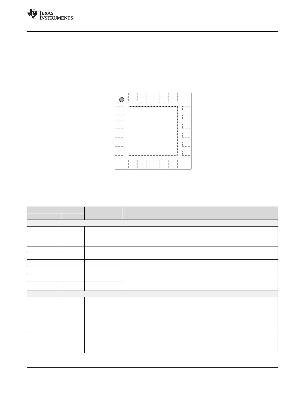
Control Logic
Power
Management
OUT0±
OUT1±
Single 2.5 V
or
Dual 2.5 V and 1.8 V
Control
Pins
Serial
Interface
SPI
or
SMBus
Lock
Indicator
OUT_MUX
100-Ÿ
Driver
100-Ÿ
Driver
LDO
2
2
Reclocker
with
Integrated
LoopFilter,
EyeMon
Data
Clock
IN_MUX
SE 75 Ÿ
Term
Cable
EQ
IN0±
2
Diff 100 Ÿ
Term
PCB
EQ
IN1±
2
VDD_LDO
Product
Folder
Order
Now
Technical
Documents
Tools &
Software
Support &
Community
Reference
Design
An IMPORTANT NOTICE at the end of this data sheet addresses availability, warranty, changes, use in safety-critical applications,
intellectual property matters and other important disclaimers. PRODUCTION DATA.
English Data Sheet: SNLS530
LMH1219
ZHCSIC9D –APRIL 2016–REVISED JUNE 2018
LMH1219 具具有有集集成成时时钟钟恢恢复复器器的的低低功功耗耗 12G UHD 自自适适应应电电缆缆均均衡衡器器
1
1 特特性性
1
• 支持 ST-2082-1(12G)、ST-2081-1(6G)、ST-424
(3G)、ST-292(HD) 和 ST-259(SD)
• 支持适用于 SMPTE 2022-5/6 的 SFF8431 (SFP+)
• 兼容 DVB-ASI 和 AES10 (MADI)
• 集成的无基准时钟恢复器锁定至 SMPTE 和 10GbE
速率:11.88Gbps、5.94Gbps、2.97Gbps、
1.485Gbps 或经 1.001 分频的子速率、270Mbps
和 10.3125Gbps
• 在输入 0 (IN0) 端具有自适应电缆均衡器
• 电缆长度 (Belden 1694A):
– 11.88Gbps (4Kp60 UHD) 时 75m
– 5.94Gbps (UHD) 时 120m
– 2.97Gbps (FHD) 时 200m
– 1.485Gbps (HD) 时 280m
– 270 Mbps (SD) 时 600m
• 输入 1 (IN1) 上具有自适应电路板走线均衡器
• 低功耗:250mW(典型值)
• 省电模式:16mW
• 集成输入回波损耗网络
• 2:1 输入多路复用,1:2 扇出输出,具有去加重功能
• 支持信号分离器模式(–6dB 启动幅值)
• 片上回路滤波器电容和眼图监视器
• 由 2.5V 单电源或片上 1.8V 稳压器供电
• 可通过控制引脚、SPI 或者 SMBus 接口进行配置
• 4mm×4mm 24 引脚 QFN 封装
• 工作温度范围:-40°C 至 +85°C
2 应应用用
• 兼容 SMPTE 的串行数字接口
• UHDTV/4K/8K/HDTV/SDTV 视频
• 广播视频路由器、交换机、分布式放大器和监视器
• 数字视频处理和编辑
• 10GbE - SDI 媒体网关
3 说说明明
LMH1219 是一款具有集成时钟恢复器的低功耗双输入
双输出自适应均衡器。该器件支持高达 11.88Gbps 的
SMPTE 视频速率以及基于 IP 传输的 10GbE 视频,
能够应用于 4K/8K 超高清 (UHD) 应用至 RTN。IN0 端
的远距离自适应电缆均衡器设计用于均衡通过 75Ω 同
轴电缆传输的数据,可在较宽的传输速率下运行,支持
的速率范围为 125Mbps 到 11.88Gbps。IN1 上的自适
应电路板走线均衡器与 SFF-8431 兼容,并且支持
SMPTE 和 10GbE 数据速率。
集成时钟恢复器可削弱高频抖动并且提供出色的信号完
整性。该器件的高输入抖动容差改善了时序裕度。时钟
恢复器内置有回路滤波器,运行时无需精准的输入基准
时钟。非破坏性眼图监视器支持实时测量串行数据,从
而简化系统调试并加速电路板调通。
凭借集成的 2:1 复用和 1:2 扇出电路,该器件能够灵活
输出多种视频信号。输出驱动器提供可编程的去加重功
能,用于补偿其输出端的电路板走线损失。集成式回波
损耗网络在所有数据传输速率下均可满足严格的
SMPTE 规范要求。LMH1219 典型的功耗值为
250mW。无输入信号时,功耗会进一步降至 16mW。
LMH1219 与 LMH1226(12G UHD 时钟恢复器)以及
LMH0324(3G 自适应电缆均衡器)引脚兼容。
器器件件信信息息
(1)
器器件件型型号号 封封装装 封封装装尺尺寸寸((标标称称值值))
LMH1219 QFN (24) 4.00mm × 4.00mm
(1) 如需了解所有可用封装,请参阅产品说明书末尾的可订购产品
附录。
简简化化框框图图


剩余55页未读,继续阅读
资源评论


不觉明了
- 粉丝: 3119
- 资源: 5348


最新资源
- 三菱PLC(Mitsubishi)通讯协议的C#实现,支持FX、Q系列的ASCII-3E、BIN-3E、FX串口格式
- 五一建模20242024
- rainy-day.jpg
- IMG_20240501_171218.jpg
- Swift-内购封装swift版本
- 经典CNN网络之ResNet 图像分类网络实战项目:7种小麦叶片病害分类(迁移学习)
- Java毕设之ssm010基于ssm的新能源汽车在线租赁管理系统+vue.rar
- Java毕设之ssm009毕业生就业信息统计系统+vue.rar
- Java毕设之ssm008医院门诊挂号系统+jsp.rar
- Java毕设之ssm007亚盛汽车配件销售业绩管理统+jsp.rar
资源上传下载、课程学习等过程中有任何疑问或建议,欢迎提出宝贵意见哦~我们会及时处理!
点击此处反馈


