没有合适的资源?快使用搜索试试~ 我知道了~
TI-UCC3972.pdf
需积分: 10 0 下载量 126 浏览量
2022-11-19
23:38:09
上传
评论 5
收藏 1.14MB PDF 举报
温馨提示
试读
25页
TI-UCC3972.pdf
资源推荐
资源详情
资源评论
UCC1972/3
UCC2972/3
UCC3972/3
DESCRIPTION
Design goals for a Cold Cathode Fluorescent Lamp (CCFL) converter used
in a notebook computer or portable application include small size, high effi
-
ciency, and low cost. The UCC3972/3 CCFL controllers provide the neces
-
sary circuit blocks to implement a highly efficient CCFL backlight power
supply in a small footprint 8 pin TSSOP package. The BiCMOS controllers
typically consume less than 1mA of operating current, improving overall
system efficiency when compared to bipolar controllers requiring 5mA to
10mA of operating current.
External parts count is minimized and system cost is reduced by integrating
such features as a feedback controlled PWM driver stage, open lamp pro
-
tection, startup delay and synchronization circuitry between the buck and
push-pull stages. The UCC3972/3 include an internal shunt regulator, al
-
lowing the part to operate with input voltages from 4.5V up to 25V. The part
supports both analog and externally generated low frequency dimming
modes of operation.
The UCC3973 adds a programmable voltage clamp at the BUCK pin. This
feature can be used to protect the transformer from overvoltage during
startup or when an open lamp occurs. Transformer voltage is controlled by
reducing duty cycle when an over-voltage is detected.
BiCMOS Cold Cathode Fluorescent Lamp Driver Controller
FEATURES
•
1mA Typical Supply Current
•
Accurate Lamp Current Control
•
Analog or Low Frequency Dimming
Capability
•
Open Lamp Protection
•
Programmable Startup Delay
•
4.5V to 25V Operation
•
PWM Frequency Synchronized to
External Resonant Tank
•
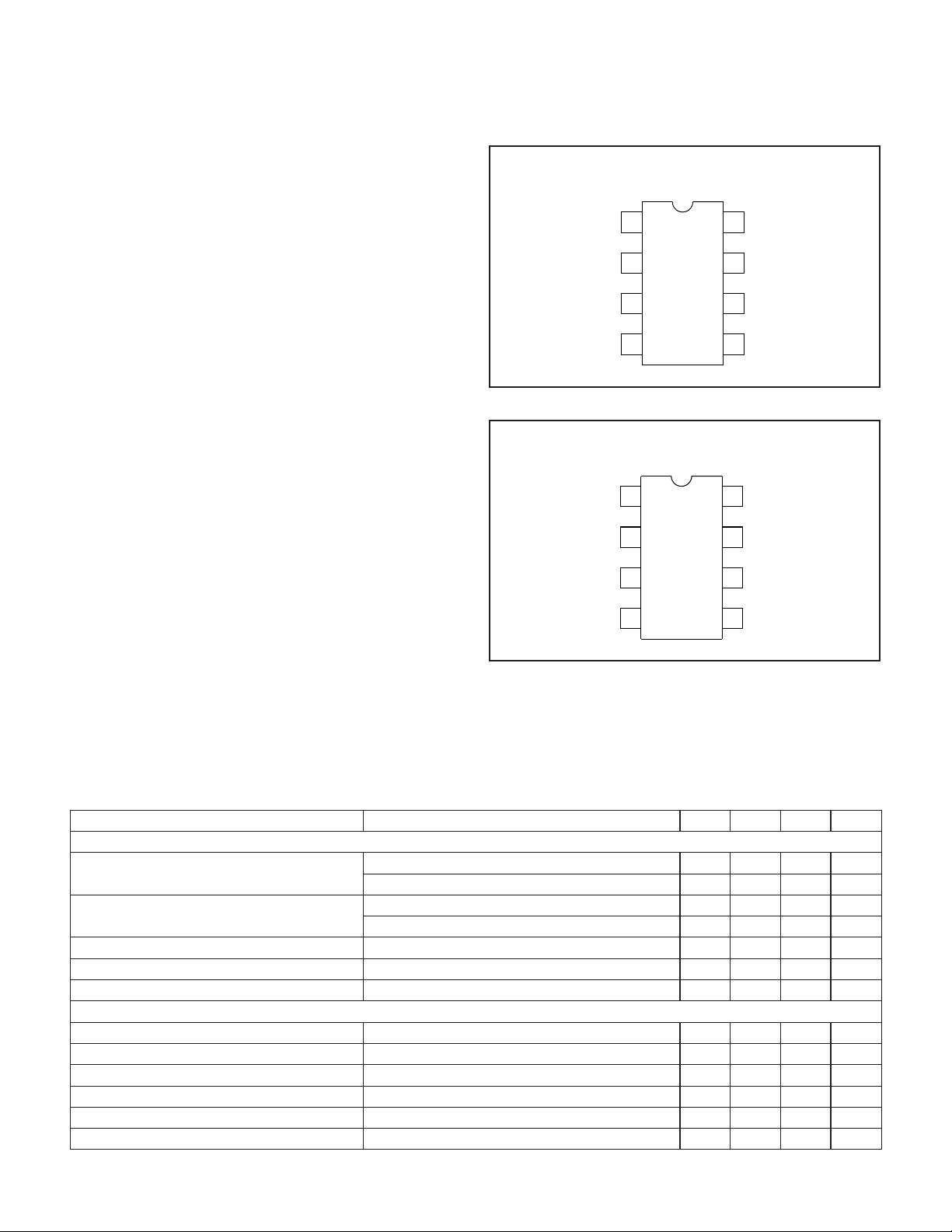
8 Pin TSSOP and SOIC Packages
Available
• Internal Voltage Clamp Protects
Transformer from Over-voltage
(UCC3973)
SLUS252C - OCTOBER 1998 - REVISED MARCH 2005
3
8
6
5
VBAT
4
2
1
7
VDD
GND
MODE
COMP
BUCK
OUT
FB
C7
0.1µF
D1 R10
R11
Q3
C5 0.1µF
L1
68µH
R6 75Ω
Q2
R2 1k
T1
C6 27pF
LAMP
HV
LAMP
LV
R3 68k
D2
R5 10k
R4 750
ANALO G
DIMMING
D
LF D
R
LF D
68k
0V-5V LOW FREQUENCY CONTROL S IGNAL
C4 33nF
LOW FREQUENCY DIMMING
C2
1µF
R1
1kΩ
C1
6.8µF
S YS TEM VO LTAG E
(4.5V TO 25V)
C3
1µF
UCC3972
UCC3973
NO INTER NAL VO LTAG E C LAMP
INTE R NAL VO LTAG E C LAMP LIMITS TR ANS FO R MER
VO LTAG E AT S TART-UP O R DUR ING F AULT
UCC3972/3
TYPICAL APPLICATION CIRCUIT
UDG-99154
2
UCC1972/3
UCC2972/3
UCC3972/3
TSSOP-8 (TOP VIEW)
PW Package
ABSOLUTE MAXIMUM RATINGS
VBAT .........................................+27V
VDD Maximum Forced Current ....................30mA
Maximum Forced Voltage ..........................17V
BUCK .................................. –5VtoVBAT
MODE .................................–0.3V to 4.0V
MODE Maximum Forced Current ..................300mA
Operating Junction Temperature ..........–55°C to +150°C
Storage Temperature ...................–65°C to +150°C
Unless otherwise indicated, currents are positive into, negative
out of the specified terminal. Pulse is defined as less than 10%
duty cycle with a maximum duration of 500ms. Consult Pack
-
aging Section of Databook for thermal limitations and consider
-
ations of packages. All voltages are referenced to GND.
GND
OUT
VDD
MODE
VBAT
BUCK
COMP
FB
1
2
3
4
8
7
6
5
CONNECTION DIAGRAMS
ELECTRICAL CHARACTERISTICS:
Unless otherwise specified these specifications hold for T
A
=0°C to +70°C for the
UC3972/3, –40°C to +85°C for the UC2972/3, and –55°C to +125°C for the UC1972/3; T
A
=T
J
; VDD=VBAT=VBUCK=12V;
MODE=OPEN. For any tests with VBAT>17V, place a 1k resistor from VBAT to VDD.
PARAMETER TEST CONDITIONS MIN TYP MAX UNITS
Input supply
VDD Supply Current VDD = 12V 1 1.5 mA
VBAT = 25V 7 10.5 mA
VBAT Supply Current VBAT = 12V 30 60
mA
VBAT = 25V 70 140 mA
VDD Regulator Turn-on Voltage I
SOURCE
= 2mA to 10mA 17 18 19 V
VDD UVLO Threshold Low to high 3.6 4 4.4 V
UVLO Threshold Hysteresis 100 200 300 mV
Output Section
Pull Down Resistance I
SINK
= 10mA to 100mA 25 50 W
Pull Up Resistance I
SOURCE
= 10mA to 100mA 25 50 W
Output Clamp Voltage VBAT = 25V, Shunt Regulator on 16 18 V
Output Low MODE = 0.5V, I
SINK
= 1mA 0.05 0.2 V
Rise Time CL = 1nF, Note 1 200 ns
Fall Time CL = 1nF, Note 1 200 ns
FB
MODE
GND
COMP
VDD
OUT
BUCK
VBAT
1
2
3
4
8
7
6
5
DIL-8 (TOP VIEW)
J, N Packages
3
UCC1972/3
UCC2972/3
UCC3972/3
ELECTRICAL CHARACTERISTICS:
Unless otherwise specified these specifications hold for T
A
=0°C to +70°C for the
UC3972/3, –40°C to +85°C for the UC2972/3, and –55°C to +125°C for the UC1972/3; T
A
=T
J
; VDD=VBAT=VBUCK=12V;
MODE=OPEN. For any tests with VBAT>17V, place a 1k resistor from VBAT to VDD.
PARAMETER TEST CONDITIONS MIN TYP MAX UNITS
Oscillator Section
Synchronizable Frequency (See Note 2.) BUCK = VBAT– 2, V
BAT
= 12V to 25V,
T
A
= –40°C to +85°C
80 - 160 kHz
BUCK = VBAT–2, V
BAT
= 12V to 25V
T
A
= –55°C to +125°C
80 - 145 kHz
Maximum Duty Cycle FB = 1V, T
A
< 0°C 84 %
FB = 1V, T
A
= 0°C to 70°C 90 95 %
Minimum Duty Cycle FB = 2V 0 %
BUCK Input Bias Current BUCK = VBAT = 12V 40 90 mA
BUCK = VBAT = 25V 80 110 mA
Zero Detect Threshold Measured at BUCK w/respect to VBAT,
VBAT=12V to 25V, T
A
< 0°C
–2.4 –1 –0.3 V
Measured at BUCK w/respect to VBAT,
VBAT=12V to 25V, T
A
= 0°C to 70°C
–2.0 –1 –0.3 V
Error Amplifier
Input Voltage COMP = 2V, T
A
=0°Cto+70°C 1.465 1.5 1.535 V
COMP = 2V 1.455 1.545 V
Line Regulation –2 2 10 mV
Input Bias Current –500 –100 nA
Open Loop Gain COMP = 0.5V to 3.0V 60 80 dB
Output High Voltage FB = 1V 3.3 3.7 4.1 V
Output Low Voltage FB = 2V 0.15 0.35 V
Output Source Current FB = 1V, COMP = 2V –1.2 –0.4 mA
Output Sink Current FB = 2V, COMP = 2V 2 4 mA
Output Source Current FB = 1V, COMP = 2V, MODE = 0.5V –1 1
mA
Output Sink Current FB = 2V, COMP = 2V, MODE = 0.5V –1 1
mA
Unity Gain Bandwidth T
J
= 25C, Note 1 2 MHz
Mode Select
Output Enable Threshold 0.85 1 1.15 V
Open Lamp Detect Enable Threshold 2.75 3 3.25 V
Mode Output Current MODE = 0.5V 15 20 25
mA
MODE Clamp Voltage MODE = OPEN 3.3 3.7 4 V
Open Lamp
Open Lamp Detect Threshold Measured at BUCK with respect to VBAT,
VBAT=12V to 25V
–8 –7 –6 V
Over-voltage Clamp Threshold (UCC3973) Measured at BUCK with respect to VBAT,
VBAT=12V to 25V, I
FB
= 100µA
–10.3 –9 –7.7 V
Note 1. Ensured by design. Not 100% tested in production.
Note 2. Oscillator operates at 2x transformer switching frequencey.
4
UCC1972/3
UCC2972/3
UCC3972/3
BUCK:Senses the voltage on the top side of the induc
-
tor feeding the resonant tank. The voltage at this point
is used to synchronize the internally generated ramp
and to detect whether an open lamp condition exists.
An open lamp condition exists when this voltage is be
-
low the specified threshold for seven clock cycles. If the
MODE pin is held below the open lamp detect enable
threshold, this protective feature is disabled.
On the UCC3973, this pin is also used to sense an
over-voltage across the transformer primary. If the volt
-
age at this pin exceeds the clamp threshold, current will
be sourced fron the FB pin.
COMP: Output of the error amplifier.Compensation
components set the bandwidth of the entire system and
are normally connected between COMP and FB. The
error amplifier averages lamp current against a fixed in
-
ternal reference. The resulting voltage on the COMP
pin is compared to an internally generated ramp, set
-
ting the PWM duty cycle. During UVLO, this pin is ac-
tively pulled low.
FB: This pin is the inverting input to the error amplifier.
On the UCC3973, current is sourced form this pin if the
clamp threshold is exceeded at the BUCK pin (see be-
low). The sourced current will reduce OUT duty cycle to
control transformer primary voltage. The source current
is disabled on the UCC3972.
GND: Ground reference for the IC.
MODE: The voltage on this pin is used to control start-up
and various modes of operation for the part (refer to the ta
-
ble in the block diagram).
When the voltage is below 1V, OUT is forced low, open
lamp detection is disabled and the error amplifier is
tri-stated.
When the voltage is between 1V and 3V, OUT is enabled
and the error amplifier output is connected to COMP. Open
lamp detection is still disabled and a constant 20 A current
is sourced from this pin. Placing an appropriate value ex
-
ternal capacitor between this pin and ground allows the
user to disable open lamp detection for a set period of time
at start-up to allow the lamp to strike.
When MODE reaches 3V, open lamp detection is enabled
and normal operation is activated.
OUT: Drives the buck regulator N-channel MOSFET. OUT
turn-on is synchronized to twice the tank resonant fre-
quency. OUT is actively pulled low when in UVLO, an
open lamp condition has been detected or MODE is less
than 1V.
VBAT:Positive input supply to power stage. This voltage is
required by internal control circuitry to provide open-lamp
detection and synchronization. Operating range is from
4.5V to 25V.
VDD: This pin connects to the battery voltage from which
the CCFL inverter will operate. If the potential on VBAT
can exceed 18V in the application, a series resistor must
be placed between VBAT and this pin (see applications
section). The voltage at the VDD pin will then be regulated
to 18V. This pin should be bypassed with a minimum ca
-
pacitance of 0.1mF.
PIN DESCRIPTIONS
0
200
400
600
800
8.7 9.2 9.7
VBAT -VBUCK
CURRENT OUT OF FB (uA)
Clamp current vs. tank voltage for UCC3973.
5
UCC1972/3
UCC2972/3
UCC3972/3
UDG-98154
*MODE Output Open Lamp
Detection
S2 Error Amplifier Output S1
<1V OFF DISABLED OPEN DISCONNECTED FROM COMP OPEN
1V< MODE< 3V ON DISABLED OPEN CONNECTED TO COMP CLOSED
>3V ON ENABLED CLOSED CONNECTED TO COMP CLOSED
8
5
3
4
2
1
7
6
VDD
20µA
+
–
+
–
1.5V
ERROR
AMP LIFIE R
S1
R
QS
R
Q
S
+
–
+
–
+
+
1.0V
7.0V
SYNC
OUTRAMP
+
0.2V
OSCILLATOR
*MO D E
SELECT
UVLO
4.0V/3.8V
3V REF
VR E F
UVLO =1
3BIT
UP-DOWN
COUNTER
S2
FROM MO DE S ELECT
OP EN LAMP DETECT
C O MP AR ATO R
ZERO DETECT
C O MP AR ATO R
UVLO
PWM
UVLO
OUTPUT OFF
(FROM MO DE S ELECT)
VDD
MO DE
COMP
FB
GND
OUT
BUCK
VDD
VBAT
18V
+
–
+
TO S3
OVER-VOLTAGE
CLAMP COMP ARATOR
S3
(ALWAYS OP EN ON UCC3972)
FROM
CLAMP
COMP
I
CLAMP
9.0V
BLOCK DIAGRAM
Introduction
Cold Cathode Fluorescent Lamps (CCFL) are frequently
used as the backlight source for Liquid Crystal Displays
(LCDs). These displays are found in numerous applica
-
tions such as notebook computers, portable instrumenta
-
tion, automotive displays, and retail terminals.
Fluorescent lamps provide superior light output effi
-
ciency, making their use ideal for power sensitive porta
-
ble applications where the backlight circuit can consume
a significant portion of the battery’s capacity. The
backlight converter must produce the high voltage
needed to strike and operate the lamp. Although CCFLs
can be operated with a DC voltage, a symmetrical AC
operating voltage is recommended to maintain the rated
life of the lamp. Sinusiodal voltage and current lamp
waveforms are also recommended to achieve optimal
electrical to light conversion and to reduce high voltage
electromagnetic interference (EMI). A topology that pro
-
vides these requirements while maintaining efficient op
-
eration is presented below.
APPLICATION INFORMATION
剩余24页未读,继续阅读
资源评论
不觉明了
- 粉丝: 3164
- 资源: 5419
上传资源 快速赚钱
- 我的内容管理 展开
- 我的资源 快来上传第一个资源
- 我的收益 登录查看自己的收益
- 我的积分 登录查看自己的积分
- 我的C币 登录后查看C币余额
- 我的收藏
- 我的下载
- 下载帮助
安全验证
文档复制为VIP权益,开通VIP直接复制
信息提交成功