没有合适的资源?快使用搜索试试~ 我知道了~
TI-UCC3912.pdf
需积分: 9 0 下载量 31 浏览量
2022-11-15
23:45:26
上传
评论 5
收藏 998KB PDF 举报
温馨提示
试读
17页
TI-UCC3912.pdf
资源推荐
资源详情
资源评论
SLUS241D − MARCH 1994 - REVISED NOVEMBER 2003
1
www.ti.com
D Integrated 0.15-Ω Power MOSFET
D 3-V to 8-V Operation
D Digital Programmable Current Limit
from 0 A to 3 A
D Electronic Circuit Breaker Function
D 1µA I
CC
When Disabled
D Programmable On-Time
D Programmable Start Delay
D Fixed 3% Duty Cycle
D Unidirectional Switch
D Thermal Shutdown
D Fault-Output Indicator
D Maximum-Output Current Can Be Set to 1 A
Above the Programmed Fault Level or to a
Full 4 A
D Power SOIC, Low-Thermal Resistance
Packaging
description
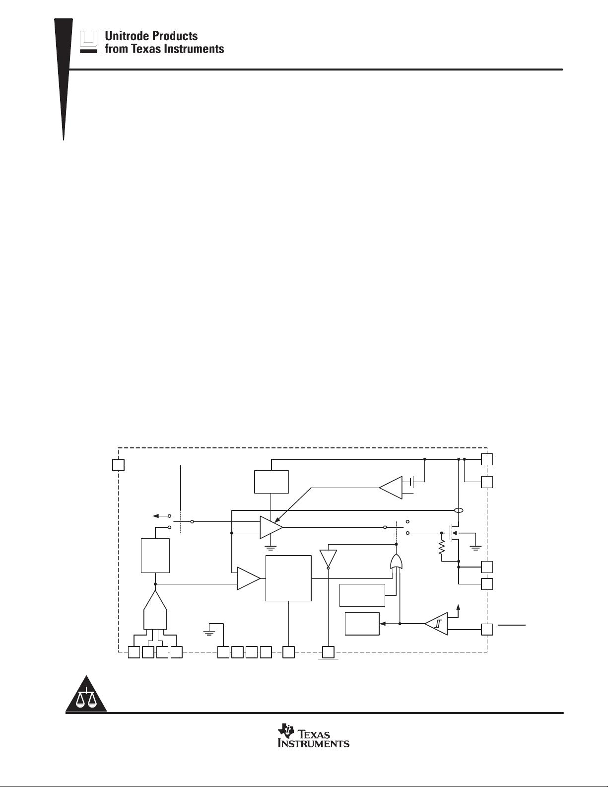
The UCC3912 family of hot swap power managers provides complete power management, hot swap capability,
and circuit breaker functions. The only component required to operate the device, other than supply bypassing,
is the fault timing capacitor, C
T
. All control and housekeeping functions are integrated, and externally
programmable. These include the fault current level, maximum output-sourcing current, maximum fault time,
and startup delay. In the event of a constant fault, the internal fixed 3% duty cycle ratio limits average output
power.
The internal 4-bit DAC allows programming of the fault level current from 0 A to 3 A with 0.25-A resolution. The
IMAX control pin sets the maximum sourcing current to 1 A above the fault level when driven low, and to a full
4 A when driven high for applications which require fast output capacitor charging.
When the output current is below the fault level, the output MOSFET is switched on with a nominal on resistance
of 0.15 Ω. When the output current exceeds the fault level, but is less than the maximum sourcing level, the
output remains switched on, but the fault timer starts charging C
T
. Once C
T
charges to a preset threshold, the
switch is turned off, and remains off for 30 times the programmed fault time. When the output current reaches
the maximum sourcing level, the MOSFET transitions from a switch to a constant current source. (continued)
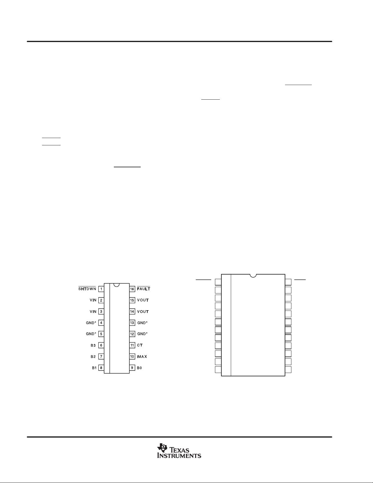
block diagram
UDG-99146
B1 B0
6 7 8
2
3
9 11 16
0 A−3 A
0.25
RES
B3 B2
5 4 13 12
CT
ON TIME
CONTROL
3% DUTY
CYCLE
+
−
THERMAL
SHUTDOWN
INTERNAL
BIAS
+
−
1
SHTDWN
14
15
1.5 V
H = OPEN
FAULT
CURRENT SENSE
+
−
+
CHARGE
PUMP
30 mV
V
OUT
REVERSE VOLTAGE
COMPARATOR
+
−
LINEAR CURRENT AMPLIFIER
1 A
ABOVE
FAULT
10IMAX
GND
HEATSINK
GND PINS
CURRENT FAULT
LEVEL 0A TO 3 A
OVERCURRENT
COMPARATOR
MAX CURRENT
LEVEL
4 A
H = 4 A VIN
VIN
VOUT
VOUT
POWER
FET
4 BIT DAC
Copyright 2003, Texas Instruments Incorporated
! "#$ ! %#&'" ($)
(#"! " !%$""! %$ *$ $! $+! !#$!
!(( ,-) (#" %"$!!. ($! $"$!!'- "'#($
$!. '' %$$!)
Please be aware that an important notice concerning availability, standard warranty, and use in critical applications of
Texas Instruments semiconductor products and disclaimers thereto appears at the end of this data sheet.
SLUS241D − MARCH 1994 - REVISED NOVEMBER 2003
2
www.ti.com
description (continued)
The UCC3912 family is designed for unidirectional current flow, emulating an ideal diode in series with the power
switch. This feature is particularly attractive in applications where many devices are powering a common bus,
such as with SCSI Termpwr.
The UCC3912 family can be put into sleep mode drawing only 1-µA of supply current. The SHTDWN
pin has
a preset threshold hysteresis which allows the user the ability to set a time delay upon startup to achieve
sequencing of power. Other features include an open drain FAULT
output indicator, thermal shutdown, under
voltage lockout, and a low thermal resistance small outline package.
absolute maximum ratings over operating free-air temperature (unless otherwise noted)
†}
VIN 8 V. . . . . . . . . . . . . . . . . . . . . . . . . . . . . . . . . . . . . . . . . . . . . . . . . . . . . . . . . . . . . . . . . . . . . . . . . . . . . . . . . . . . . . . .
FAULT
sink current 50 mA. . . . . . . . . . . . . . . . . . . . . . . . . . . . . . . . . . . . . . . . . . . . . . . . . . . . . . . . . . . . . . . . . . . . . . .
FAULT
voltage -0.3 to V
IN
. . . . . . . . . . . . . . . . . . . . . . . . . . . . . . . . . . . . . . . . . . . . . . . . . . . . . . . . . . . . . . . . . . . . . . . .
Output current Self Limiting. . . . . . . . . . . . . . . . . . . . . . . . . . . . . . . . . . . . . . . . . . . . . . . . . . . . . . . . . . . . . . . . . . . . . .
Input voltage
(B0, B1, B2, B3, IMAX, SHTDWN
) -0.3 to V
IN
. . . . . . . . . . . . . . . . . . . . . . . . . . . . . . . . . . . . . . . . . . . . . . . . . . . .
Storage temperature range, T
stg
-65°C to 150°C. . . . . . . . . . . . . . . . . . . . . . . . . . . . . . . . . . . . . . . . . . . . . . . . . . . .
Operating junction temperature range, T
J
-55°C to 150°C. . . . . . . . . . . . . . . . . . . . . . . . . . . . . . . . . . . . . . . . . . . .
Lead temperature (soldering, 10 sec.) 300°C. . . . . . . . . . . . . . . . . . . . . . . . . . . . . . . . . . . . . . . . . . . . . . . . . . . . . . .
†
Stresses beyond those listed under “absolute maximum ratings” may cause permanent damage to the device. These are stress ratings only, and
functional operation of the device at these or any other conditions beyond those indicated under “recommended operating conditions” is not
implied. Exposure to absolute-maximum-rated conditions for extended periods may affect device reliability.
‡
Currents are positive into, negative out of the specified terminal. Consult Packaging Section of the Interface Products Data book (TI Literature
Number SLUD002) for thermal limitations and considerations of packages.
package information
DIL-16, SOIC-16
N, DP Package
(TOP VIEW)
TSSOP-24,
PWP Package
(TOP VIEW)
*Pin 5 serves as lowest impedance to the electrical
ground; Pins 4, 12, and 13 serve as heat sink/ground.
These pins should be connected to large etch areas to
help dissipate heat. For N package, pins 4, 12, and 13
are N/C.
*Pin 9 serves as lowest impedance to the electrical ground;
other GND pins serve as heat sink/ground. These pins should
be connected to large etch areas to help dissipate heat.
B3
VOUT
GND*
GND*
FAULT
N/C
EGND*
GND*
GND*
VIN
VIN
GND*
SHTDWN
GND*
B2
GND*
GND*
CT
12
11
10
9
8
7
6
5
4
3
2
1
13
14
15
16
17
18
19
20
21
22
23
24
IMAX
N/C
VOUT
B1 B0
GND*
SLUS241D − MARCH 1994 - REVISED NOVEMBER 2003
3
www.ti.com
electrical characteristics, these specifications apply for T
A
= −40°C to 85°C for the UCC2912;
T
A
= 0°C to 70°C for the UCC3912, VIN = 5 V, IMAX = 0.4 V, SHTDWN = 2.4 V
(unless otherwise stated)
supply section
PARAMETER TEST CONDITIONS MIN TYP MAX UNITS
Voltage input range 3.0 8.0 V
Supply current 1.0 2.0 mA
Sleep mode current SHTDWN = 0.2 V 0.5 5.0 µA
NOTE 1: All voltages are with respect to ground. Current is positive into and negative out of the specified terminal.
output section
PARAMETER TEST CONDITIONS MIN TYP MAX UNITS
I
OUT
= 1 A 0.15 0.22 V
I
OUT
= 2 A 0.3 0.45 V
Voltage drop
I
OUT
= 3 A 0.45 0.68 V
Voltage drop
I
OUT
= 1A, VIN = 3 V 0.17 0.27 V
I
OUT
= 2 A, VIN = 3 V 0.35 0.56 V
I
OUT
= 3 A, VIN = 3 V 0.5 0.8 V
Reverse leakage current V
IN
< V
OUT
, SHTDWN = 0.2 V, V
OUT
= 5 V 5 20 µA
Initial startup time See Note 2 100 µs
Short circuit response See Note 2 100 ns
Thermal shutdown See Note 2 170 °C
Thermal hysteresis See Note 2 10 °C
NOTE 1: All voltages are with respect to ground. Current is positive into and negative out of the specified terminal.
NOTE 2: Ensured by design. Not production tested.
DAC section
PARAMETER TEST CONDITIONS MIN TYP MAX UNITS
Output leakage Code = 0000−0011 0 20 µA
Code = 0100 0.1 0.25 0.45 A
Code = 0101 0.25 0.50 0.75 A
Code = 0110 0.5 0.75 1.0 A
Code = 0111 0.75 1.00 1.25 A
Code = 1000 1.0 1.25 1.5 A
Trip current
Code = 1001 1.25 1.50 1.75 A
Trip current
Code = 1010 1.5 1.75 2.0 A
Code = 1011 1.7 2.00 2.3 A
Code = 1100 1.9 2.25 2.58 A
Code = 1101 2.1 2.50 2.9 A
Code = 1110 2.3 2.75 3.2 A
Code = 1111 2.5 3.0 3.5 A
Maximum output current Code = 0000 to 0011 0.02 mA
Maximum output current over trip
UCC2912 Code = 0100 to 1111, I
MAX
= 0 V 0.5 1.0 2.0 A
Maximum output current over trip
(current source mode)
UCC3912 Code = 0100 to 1111, I
MAX
= 0 V 0.5 1.0 1.8 A
Maximum output current (current source mode) Code = 0100 to 1111, I
MAX
= 2.4 V 3.0 4.0 5.2 A
NOTE 1: All voltages are with respect to ground. Current is positive into and negative out of the specified terminal.
SLUS241D − MARCH 1994 - REVISED NOVEMBER 2003
4
www.ti.com
electrical characteristics, these specifications apply for T
A
= −40°C to 85°C for the UCC2912;
T
A
= 0°C to 70°C for the UCC3912, VIN = 5 V, IMAX = 0.4 V, SHTDWN = 2.4 V
(unless otherwise stated)
timer section
PARAMETER TEST CONDITIONS MIN TYP MAX UNITS
CT charge current V
CT
= 1.0 V −45.0 -36.0 −22.0 µA
CT discharge current
UCC2912 V
CT
= 1.0 V 0.72 1.20 1.57 µA
CT discharge current
UCC3912 V
CT
= 1.0 V 0.72 1.20 1.50 µA
Output duty cycle V
OUT
= 0 V 2.0 3.0 6.0 %
CT fault threshold 1.3 1.5 1.7 V
CT reset threshold 0.4 0.5 0.6 V
NOTE 1: All voltages are with respect to ground. Current is positive into and negative out of the specified terminal.
shutdown section
PARAMETER TEST CONDITIONS MIN TYP MAX UNITS
Shutdown threshold 1.1 1.5 1.9 V
Shutdown hysteresis 100 mV
Input current SHTDWN = 1 V 100 500 nA
fault output section
PARAMETER TEST CONDITIONS MIN TYP MAX UNITS
Output leakage current 500 nA
Low level output voltage I
OUT
= 10 mA 0.4 0.8 V
TTL input dc characteristics section
PARAMETER TEST CONDITIONS MIN TYP MAX UNITS
TTL input voltage high (can be connected to V
IN
) 2.0 V
TTL input voltage low 0.8 V
TTL input high current V
IH
= 2.4 V 3 10 µA
TTL input low current V
IL
= 0.4 V 1 µA
NOTE 1: All voltages are with respect to ground. Current is positive into and negative out of the specified terminal.
pin description
B0−B3: These pins provide digital input to the DAC which sets the fault current threshold. They can be used
to provide a digital soft-start, adaptive current limiting.
CT: A capacitor connected to ground sets the maximum fault time. The maximum fault time must be more than
the time to charge the external capacitance in one cycle. The maximum fault time is defined as
FAULT = 27.8 × 10
3
× CT. Once the fault time is reached the output will shutdown for a time given by:
T
SD
= 833 × 10
3
× CT, this equates to a 3% duty cycle.
FAULT
: Open drain output which pulls low upon any condition which causes the output to open: fault, thermal
shutdown, or shutdown.
IMAX: When this pin is set to logic low the maximum sourcing current will always be 1 A above the programmed
fault level. When set to logic high, the maximum sourcing current will be a constant 4 A for applications which
require fast charging of load capacitance.
剩余16页未读,继续阅读
资源评论
不觉明了
- 粉丝: 3164
- 资源: 5429
上传资源 快速赚钱
- 我的内容管理 展开
- 我的资源 快来上传第一个资源
- 我的收益 登录查看自己的收益
- 我的积分 登录查看自己的积分
- 我的C币 登录后查看C币余额
- 我的收藏
- 我的下载
- 下载帮助
安全验证
文档复制为VIP权益,开通VIP直接复制
信息提交成功