TI-LMP92018.pdf
需积分: 10 162 浏览量
2022-11-27
16:41:21
上传
评论 4
收藏 1MB PDF 举报

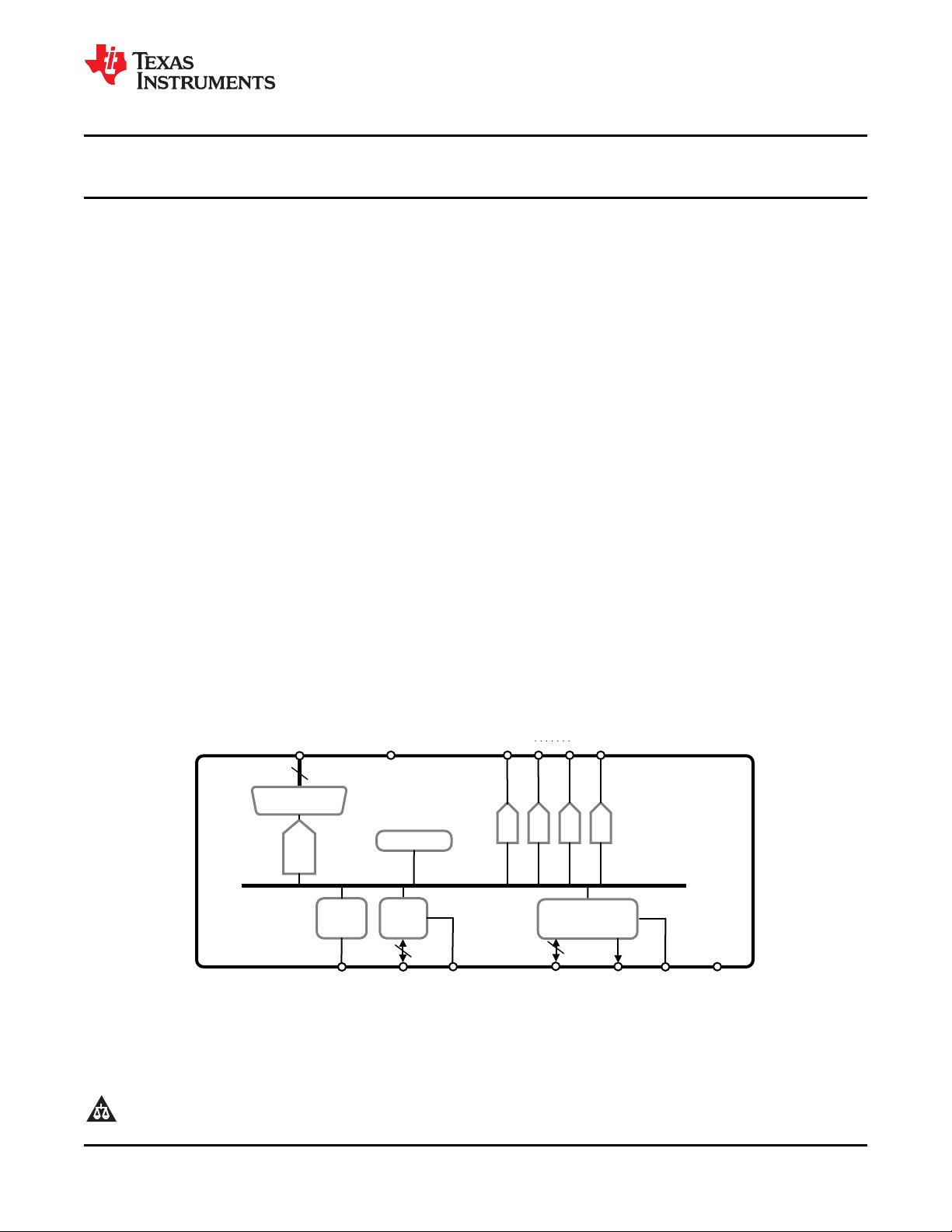
Multiplexer
ADC
LMP92018
8
Temp. Sensor
DAC
DAC
DAC
DAC
Int/Ext
Ref
4
SPI
Interface
12
GPIO
REF
GPIO[11:0]
CSB
SCLK
DIN
DOUT
OUT3
OUT0
IN[7:0]
DRDYB
VGPIO
VIO
VDD
GND
LMP92018
www.ti.com
SNAS514B –NOVEMBER 2011–REVISED MAY 2013
LMP92018 Analog System Monitor and Controller
Check for Samples: LMP92018
1
FEATURES
APPLICATIONS
2
• 8 ANALOG VOLTAGE MONITORING
• Communication Infrastructure
CHANNELS
• System Monitoring and Control
– 10-Bit ADC with Programmable Input MUX
• Industrial Monitoring and Control
– Internal/External Reference
DESCRIPTION
– Tolerates High-Source Impedance at Lower
LMP92018 is a complete analog monitoring and
Sampling Rates
control circuit which integrates an eight channel 10-bit
• 4 PROGRAMMABLE ANALOG VOLTAGE
Analog-to-Digital Converter (ADC), four 10-bit Digital-
OUTPUTS
to-Analog Converters (DACs), an internal reference,
– Four 10-Bit DACs
an internal temperature sensor, a12-bit GPIO port,
and a 10MHz SPI interface.
– Internal/External Reference
– Drives Loads up to 1nF
The eight channels of the ADC can be used to
monitor rail voltages, current sense amplifier outputs,
• VOLTAGE REFERENCE
health monitors or sensors while the four DACs can
– User-Selectable Source: External or Internal
be used to control PA (Power Amplifier) bias points,
– Internal Reference 2.5V
control actuators, potentiometers, etc.
• TEMPERATURE SENSOR
Both the ADC and DACs can use either the internal
– ±2.5°C Accuracy
2.5V reference or an external reference
independently allowing for flexibility in system design.
• 12-BIT GPIO PORT
– Each Bit Individually Programmable
The built-in digital temperature sensor enables
accurate (±2.5°C) local temperature measurement
– User-Selectable Rail
whose value is captured in the user accessible
• SPI-COMPATIBLE BUS
register.
– User-Selectable Rail
Block Diagram
1
Please be aware that an important notice concerning availability, standard warranty, and use in critical applications of
Texas Instruments semiconductor products and disclaimers thereto appears at the end of this data sheet.
2All trademarks are the property of their respective owners.
PRODUCTION DATA information is current as of publication date.
Copyright © 2011–2013, Texas Instruments Incorporated
Products conform to specifications per the terms of the Texas
Instruments standard warranty. Production processing does not
necessarily include testing of all parameters.


剩余33页未读,继续阅读
资源评论


