没有合适的资源?快使用搜索试试~ 我知道了~
TI-DS90UB902Q-Q1.pdf

FPD-Link解串器
资源推荐
资源详情
资源评论


DS90UB901Q, DS90UB902Q
www.ti.com.cn
ZHCSB01E –JUNE 2010–REVISED APRIL 2013
具具有有双双向向控控制制通通道道的的 DS90UB901Q/DS90UB902Q 10 - 43MHz 14 位位彩彩色色
平平面面显显示示器器 (FPD) - 连连接接 III 串串化化器器和和解解串串器器
查查询询样样品品: DS90UB901Q, DS90UB902Q
1
特特性性
说说明明
2
• 10MHz 至至 43MHz 输输入入并并行行端端口口时时钟钟 (PCLK) 支支持持
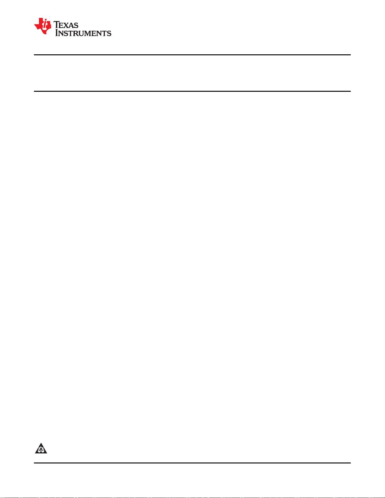
DS90UB901Q/DS90UB902Q 芯片组为一个单个差分
对上的数据传输提供了支持高速正向通道和一个双向控
• 160Mbps 至至 688Mbps 数数据据吞吞吐吐量量
制通道的 FPD 连接 III 接口。 串化器/解串器对针对汽
• 单单个个差差分分对对互互连连
车摄像头系统与主机控制器/电子控制单元 (ECU) 之间
• 具具有有 I
2
C 支支持持的的双双向向控控制制接接口口通通道道
的直接连接。 主传输系统在单个高速串行数据流上发
• 具具有有 DC 平平衡衡编编码码的的嵌嵌入入式式时时钟钟以以支支持持 AC 耦耦合合互互
连连
送 16 位图像数据,连同一个支持 I
2
C 的低延迟双向控
• 能能够够驱驱动动长长达达 10 米米的的屏屏蔽蔽双双绞绞线线
制通道传输。 包括在 16 位有效负载之内的是一个针
对 CRC(循环冗余校验)的可选数据完整性选项以监
• I
2
C 兼兼容容串串行行接接口口
控传输链路错误。 使用德州仪器 (TI) 嵌入式时钟技术
• 单单个个硬硬件件器器件件寻寻址址引引脚脚
可在一个单个差分对上实现透明全双工通信,从而在不
• 针针对对数数据据完完整整性性检检查查的的带带有有 CRC((循循环环冗冗余余校校验验))
的的 16 位位数数据据有有效效载载荷荷
依赖于视频消隐间隔的情况下携带不对称双向控制信
• 多多达达 6 个个可可编编程程通通用用输输入入输输出出 (GPIO)
息。 这个单个串行数据流通过消除并行数据与时钟路
• LOCK((锁锁定定))输输出出报报告告,,以以及及 AT-SPEED
径间的偏差,简化了印刷电路板 (PCB) 走线和电缆上
BIST((全全速速内内置置自自检检))诊诊断断特特性性以以验验证证连连接接完完整整性性
的宽数据总线传输。 这样,通过限制数据路径的宽
• 集集成成端端接接电电阻阻器器
度,大大节省了系统成本,相应地减少了 PCB 层数、
• 1.8V 或或 3.3V 兼兼容容并并行行数数据据接接口口
电缆宽度以及连接器尺寸和引脚数量。
• 1.8V 单单电电源源
此外,解串器输入提供均衡控制来补偿较长距离介质所
• 符符合合 ISO 10605 静静电电放放电电 (ESD) 以以及及 IEC 61000-
造成的损耗。 内部 DC 均衡编码/解码被用来支持 AC
4-2 ESD 标标准准
耦合互连。
• 汽汽车车应应用用级级产产品品::符符合合 AEC-Q100 2 级级要要求求
一个串化器待机功能提供了一个支持远程唤醒功能的低
• 温温度度范范围围::-40°C 至至 +105°C
节能模式,此模式用于远程器件的信号传输。
• 解解串串器器上上无无需需基基准准时时钟钟
• 可可编编程程接接收收均均衡衡
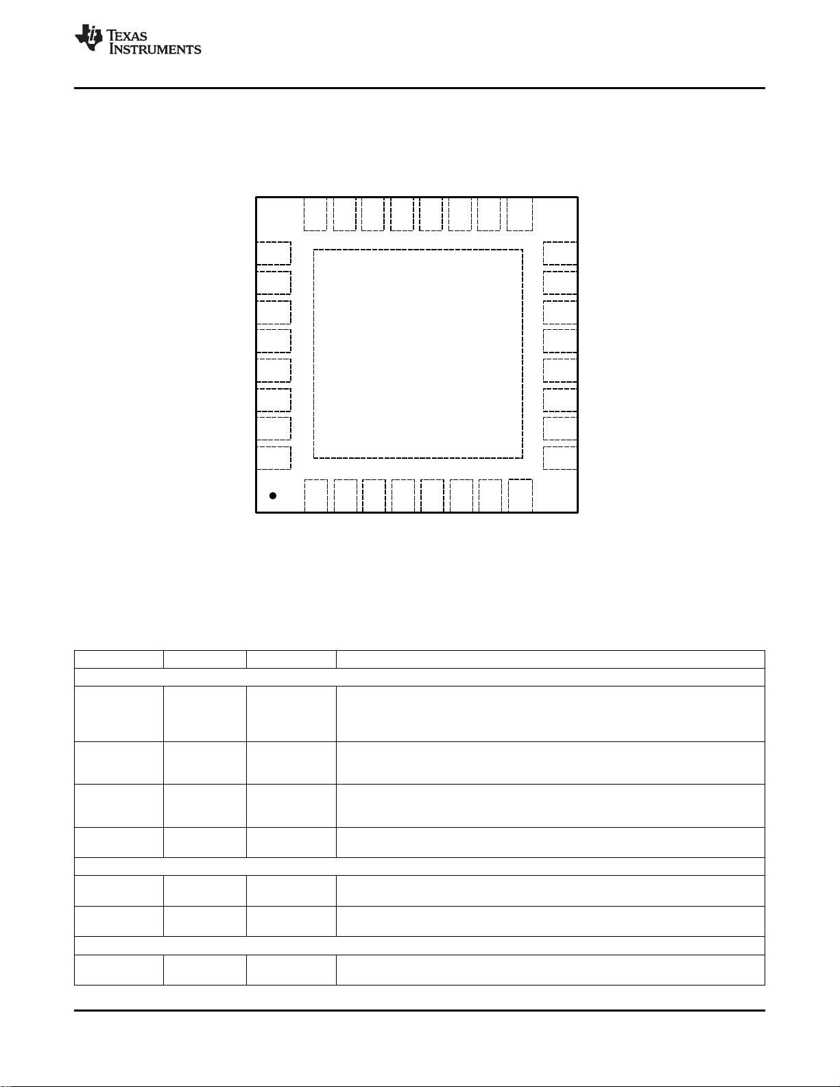
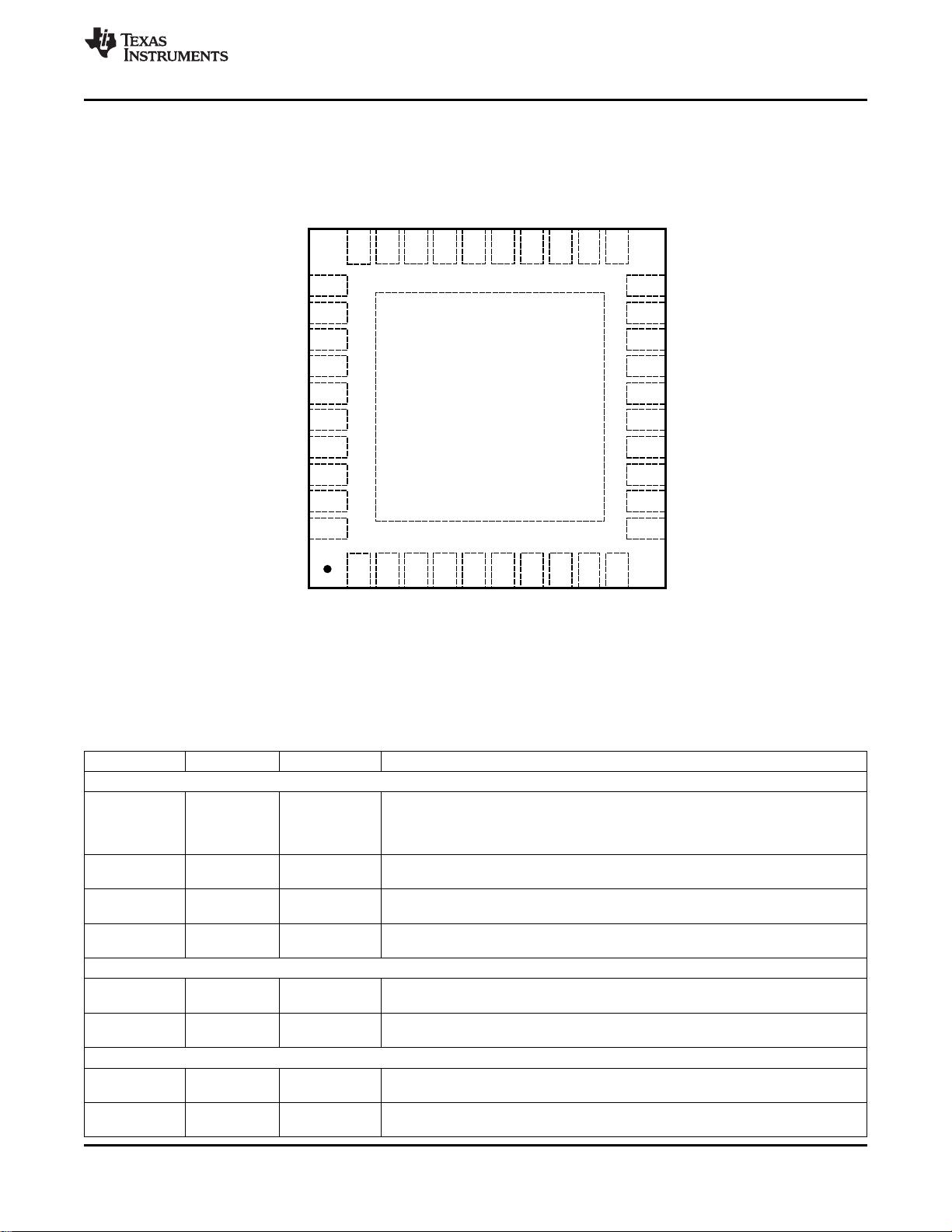
此串化器采用 32 引脚超薄型四方扁平无引线
• 电电磁磁干干扰扰 (EMI) / 电电磁磁兼兼容容性性 (EMC) 迁迁移移
(WQFN)(5mm x 5mm) 封装,而解串器采用 40 引脚
– DES 可可编编程程展展频频 (SSCG) 输输出出
WQFN (6mm x 6mm) 封装。
– DES 接接收收器器交交错错输输出出
应应用用范范围围
• 汽汽车车视视觉觉系系统统
• 后后视视、、侧侧视视摄摄像像头头
• 车车道道偏偏离离报报警警
• 辅辅助助泊泊车车
• 盲盲点点视视野野
1
Please be aware that an important notice concerning availability, standard warranty, and use in critical applications of
Texas Instruments semiconductor products and disclaimers thereto appears at the end of this data sheet.
2All trademarks are the property of their respective owners.
PRODUCTION DATA information is current as of publication date.
Copyright © 2010–2013, Texas Instruments Incorporated
Products conform to specifications per the terms of the Texas
Instruments standard warranty. Production processing does not English Data Sheet: SNLS322
necessarily include testing of all parameters.

FPD-Link III
Bidirectional
Control Channel
Image
Sensor
ECU Module
DIN[13:0]
HS, VS
SDA
SCL
DOUT-
RIN-
DOUT+
RIN+
Camera Unit
14
YUV/RGB
HSYNC
VSYNC
PCLK
Pixel Clock
SDA
SCL
Microcontroller
ROUT[13:0]
HS, VS
SDA
SCL
PCLK
14
YUV/RGB
HSYNC
VSYNC
Pixel Clock
SDA
SCL
Camera Data
DS90UB902Q
Deserializer
DS90UB901Q
Serializer
GPI/O
GPIO[1:0]
2
GPI/O
2
GPIO[1:0]
Camera Data
PCLK
DS90UB901Q - SERIALIZER
Clock
Gen
Timing
and
Control
DOUT-
R
T
RIN-
DS90UB902Q - DESERIALIZER
DOUT+
RIN+
Timing
and
Control
LOCK
PCLK
Input Latch
FIFO
Decoder
SDA
16
R
OUT
[13:0] HS, VS
Encoder
Serializer
PLL
I
2
C Controller
SCL
Encoder
FIFO
Encoder
Decoder
Deserializer
Decoder
Output Latch
Clock
Gen
CDR
SDA
SCL
R
T
R
T
R
T
D
IN
[13:0] HS, VS
16
GPIO [1:0]
2
PDB
MODE
ID[x]
GPIO [1:0]
2
PDB
MODE
ID[x]
PASS
BISTEN
I
2
C Controller
Microcontroller/
ECU
DeserializerSerializer
Image
Sensor
FPD-Link III
Bidirectional
Control Channel
Bidirectional
Control Bus
Bidirectional
Control Bus
Parallel
Data In
16
2
2
Parallel
Data Out
16
DS90UB902Q
DS90UB901Q
DS90UB901Q, DS90UB902Q
ZHCSB01E –JUNE 2010–REVISED APRIL 2013
www.ti.com.cn
These devices have limited built-in ESD protection. The leads should be shorted together or the device placed in conductive foam
during storage or handling to prevent electrostatic damage to the MOS gates.
Typical Application Diagram
Figure 1. Typical Application Circuit
Block Diagrams
Figure 2. Block Diagram
Figure 3. Application Block Diagram
2 Copyright © 2010–2013, Texas Instruments Incorporated

1 2 3 4 5 6 7
8
9
24 23 22 21 20 19 18 17
DS90B901Q
Serializer
32-Pin WQFN
(Top View)
V
DDIO
V
DDD
DIN[8]
DIN[9]
DIN[10]
DIN[11]
DIN[13]
DIN[12]
DIN[7]
DIN[6]
DIN[5]
DIN[4]
DIN[3]/GPIO[5]
DIN[2]/GPIO[4]
DIN[1]/GPIO[3]
DIN[0]/GPIO[2]
GPIO[1]
GPIO[0]
V
DDCML
V
DDT
V
DDPLL
PDB
DOUT-
DOUT+
HSYNC
VSYNC
PCLK
SCL
SDA
ID[x]
RES
MODE
DAP = GND
10
11
12
13
14
15
16
32
31
30
29
28
27
26
25
DS90UB901Q, DS90UB902Q
www.ti.com.cn
ZHCSB01E –JUNE 2010–REVISED APRIL 2013
DS90UB901Q Pin Diagram
Serializer - DS90UB901Q
32 Pin WQFN (Top View)
See Package Number RTV0032A
DS90UB901Q SERIALIZER PIN DESCRIPTIONS
Pin Name Pin No. I/O, Type Description
LVCMOS PARALLEL INTERFACE
DIN[13:0] 32, 31, 30, 29, Inputs, Parallel data inputs.
27, 26, 24, 23, LVCMOS
22, 21, 20, 19, w/ pull down
18, 17
HSYNC 1 Inputs, Horizontal SYNC Input
LVCMOS
w/ pull down
VSYNC 2 Inputs, Vertical SYNC Input
LVCMOS
w/ pull down
PCLK 3 Input, LVCMOS Pixel Clock Input Pin. Strobe edge set by TRFB control register.
w/ pull down
GENERAL PURPOSE INPUT OUTPUT (GPIO)
DIN[3:0]/ 20, 19, 18, 17 Input/Output, DIN[3:0] general-purpose pins can be individually configured as either inputs or
GPIO[5:2] LVCMOS outputs; used to control and respond to various commands.
GPIO[1:0] 16, 15 Input/Output, General-purpose pins can be individually configured as either inputs or outputs; used
LVCMOS to control and respond to various commands.
BIDIRECTIONAL CONTROL BUS - I
2
C COMPATIBLE
Input/Output, Clock line for the bidirectional control bus communication
SCL 4
Open Drain SCL requires an external pull-up resistor to V
DDIO
.
Copyright © 2010–2013, Texas Instruments Incorporated 3

DS90UB901Q, DS90UB902Q
ZHCSB01E –JUNE 2010–REVISED APRIL 2013
www.ti.com.cn
DS90UB901Q SERIALIZER PIN DESCRIPTIONS (continued)
Pin Name Pin No. I/O, Type Description
Input/Output, Data line for the bidirectional control bus communication
SDA 5
Open Drain SDA requires an external pull-up resistor to V
DDIO
.
I
2
C Mode select
MODE = L, Master mode (default); Device generates and drives the SCL clock line.
Device is connected to slave peripheral on the bus. (Serializer initially starts up in
Input, LVCMOS
MODE 8 Standby mode and is enabled through remote wakeup by Deserializer)
w/ pull down
MODE = H, Slave mode; Device accepts SCL clock input and attached to an I
2
C
controller master on the bus. Slave mode does not generate the SCL clock, but uses
the clock generated by the Master for the data transfers.
Device ID Address Select
ID[x] 6 Input, analog
Resistor to Ground and 10 kΩ pull-up to 1.8V rail. See Table 3
CONTROL AND CONFIGURATION
Power down Mode Input Pin.
PDB = H, Serializer is enabled and is ON.
Input, LVCMOS
PDB 9 PDB = L, Serailizer is in Power Down mode. When the Serializer is in Power Down,
w/ pull down
the PLL is shutdown, and IDD is minimized. Programmed control register data are
NOT retained and reset to default values
Input, LVCMOS Reserved.
RES 7
w/ pull down This pin MUST be tied LOW.
FPD-LINK III INTERFACE
Input/Output, Non-inverting differential output, bidirectional control channel input. The interconnect
DOUT+ 13
CML must be AC Coupled with a 100 nF capacitor.
DOUT- 12 Input/Output, Inverting differential output, bidirectional control channel input. The interconnect must
CML be AC Coupled with a 100 nF capacitor.
POWER AND GROUND
VDDPLL 10 Power, Analog PLL Power, 1.8V ±5%
VDDT 11 Power, Analog Tx Analog Power, 1.8V ±5%
VDDCML 14 Power, Analog CML & Bidirectional Channel Driver Power, 1.8V ±5%
VDDD 28 Power, Digital Digital Power, 1.8V ±5%
Power, Digital Power for I/O stage. The single-ended inputs and SDA, SCL are powered from V
DDIO
.
VDDIO 25
V
DDIO
can be connected to a 1.8V ±5% or 3.3V ±10%
Ground, DAP DAP must be grounded. DAP is the large metal contact at the bottom side, located at
VSS DAP the center of the WQFN package. Connected to the ground plane (GND) with at least
9 vias.
4 Copyright © 2010–2013, Texas Instruments Incorporated

2 3 4 5 6 7 8 9
1
10
31
39
38
37
36
35
34
33
32
12
13
14
15
16
17
18
19
20
40
DS90B902Q
Deserializer
40-Pin WQFN
(Top View)
HSYNC
VSYNC
PCLK
SCL
SDA
ID[x]
PASS
V
DDCML
PDB
RES/CMLOUTP
RIN+
RIN-
V
DDPLL
RES/CMLOUTN
BISTEN
RES
MODE
V
DDSSCG
V
DDIO3
ROUT[13]
ROUT[12]
ROUT[4]
ROUT[5]
ROUT[6]
ROUT[7]
V
DDIO2
ROUT[8]
ROUT[9]
V
DDD
ROUT[10]
ROUT[11]
V
DDR
LOCK
GPIO[0]
GPIO[1]
V
DDIO1
ROUT[0]/GPIO[2]
ROUT[1]/GPIO[3]
ROUT[2]/GPIO[4]
29 28 27 26 25 24 23 22
30
21
ROUT[3]/GPIO[5]
DAP = GND
11
DS90UB901Q, DS90UB902Q
www.ti.com.cn
ZHCSB01E –JUNE 2010–REVISED APRIL 2013
DS90UB902Q Pin Diagram
Deserializer - DS90UB902Q
40 Pin WQFN (Top View)
See Package Number RTA0040A
DS90UB902Q DESERIALIZER PIN DESCRIPTIONS
Pin Name Pin No. I/O, Type Description
LVCMOS PARALLEL INTERFACE
ROUT[13:0] 9, 10, 11, 12, Outputs, Parallel data outputs.
14, 15, 17, 18, LVCMOS
19, 20, 21, 22,
23, 24
HSYNC 7 Output, Horizontal SYNC Output
LVCMOS
VSYNC 6 Output, Vertical SYNC Output
LVCMOS
Output, Pixel Clock Output Pin.
PCLK 5
LVCMOS Strobe edge set by RRFB control register.
GENERAL PURPOSE INPUT OUTPUT (GPIO)
ROUT[3:0] / Input/Output, ROUT[3:0] general-purpose pins can be individually configured as either inputs or
21, 22, 23, 24
GPIO[5:2] LVCMOS outputs; used to control and respond to various commands.
Input/Output, General-purpose pins can be individually configured as either inputs or outputs; used
GPIO[1:0] 26, 27
LVCMOS to control and respond to various commands.
BIDIRECTIONAL CONTROL BUS - I
2
C COMPATIBLE
Input/Output, Clock line for the bidirectional control bus communication
SCL 3
Open Drain SCL requires an external pull-up resistor to V
DDIO
.
Input/Output, Data line for bidirectional control bus communication
SDA 2
Open Drain SDA requires an external pull-up resistor to V
DDIO
.
Copyright © 2010–2013, Texas Instruments Incorporated 5
剩余49页未读,继续阅读
资源评论

- m0_745259962023-02-02#完美解决问题 #运行顺畅 #内容详尽 #全网独家 #注释完整
- qq_335607272023-02-02#完美解决问题 #运行顺畅 #内容详尽 #全网独家 #注释完整
不觉明了
- 粉丝: 701
- 资源: 4046

上传资源 快速赚钱
我的内容管理 收起
我的资源 快来上传第一个资源
我的收益
登录查看自己的收益我的积分 登录查看自己的积分
我的C币 登录后查看C币余额
我的收藏
我的下载
下载帮助

会员权益专享
安全验证
文档复制为VIP权益,开通VIP直接复制
