TI-DS90UB935-Q1.pdf
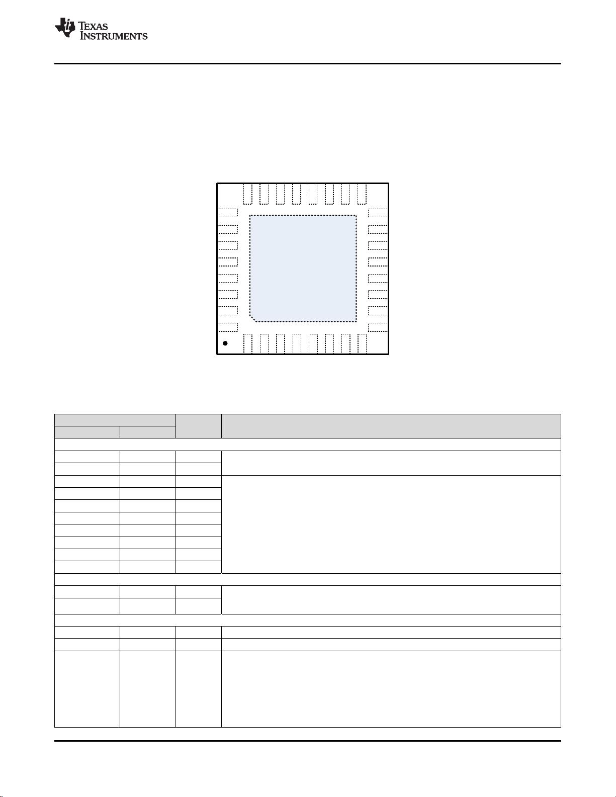
Image
Signal
Processor
(ISP)
Full HD
Image Sensor
FPD-Link III
(over Coax or STP)
DS90UB935-Q1
Serializer
DS90UB936-Q1
Deserializer
DOUT+/-
RIN+/-
MIPI CSI-2
D3P/N
CLKP/N
D2P/N
D1P/N
D0P/N
I2C
HS-GPIO
MIPI CSI-2
D3P/N
CLKP/N
D2P/N
D1P/N
D0P/N
I2C
HS-GPIO
Product
Folder
Order
Now
Technical
Documents
Tools &
Software
Support &
Community
An IMPORTANT NOTICE at the end of this data sheet addresses availability, warranty, changes, use in safety-critical applications,
intellectual property matters and other important disclaimers. PRODUCTION DATA.
English Data Sheet: SNLS605
DS90UB935-Q1
ZHCSIJ2 –JULY 2018
DS90UB935-Q1 具具有有 CSI-2 接接口口的的 FPD-Link III 3Gbps 串串行行器器
1
1 特特性性
1
• 符合面向汽车应用的 AEC-Q100 标准:
– 器件温度等级 2:环境工作温度范围为 –40°C
至 +105°C
• 符合 ISO 10605 和 IEC 61000-4-2 ESD 标准
• 同轴电缆供电 (PoC) 兼容收发器
• 3Gbps 级串行器支持高速传感器
• 符合 D-PHY v1.2 和 CSI-2 v1.3 标准的系统接口
– 高达 2.528Gbps 的 CSI-2 带宽
– 支持多达四个虚拟通道
• 精密多传感器时钟和同步
• 灵活的可编程输出时钟发生器
• 高级数据保护和诊断,包括 CRC 数据保护、传感
器数据完整性检查、I2C 写保护、电压和温度测
量、可编程警报器以及线路故障检测
• 支持单端同轴或屏蔽双绞线 (STP) 电缆
• 超低延迟双向 I2C 和 GPIO 控制通道支持从 ECU
侧进行 ISP 控制,
• 1.8V 单电源
• 低功耗(0.25W 典型值)
• 兼容 DS90UB936-Q1、DS90UB954-Q1、
DS90UB960-Q1、DS90UB934-Q1、
DS90UB914A-Q1 解串器
• 宽温度范围:–40°C 至 105°C
• 小型 5mm × 5mm VQFN 封装和 PoC 解决方案尺
寸,适合紧凑型摄像头模块设计
2 应应用用
• 汽车驾驶员辅助系统 (ADAS)
– 环视系统 (SVS)
– 摄像头监控系统 (CMS)
– 前视摄像头 (FC)
– 驾驶员监控系统 (DMS)
– 后视摄像头 (RVC)
– 汽车卫星雷达和激光雷达模块
– 飞行时间 (ToF) 传感器
• 安防和监控摄像头
• 工业和医疗成像
3 说说明明
DS90UB935-Q1 串行器是 TI FPD-Link III 器件系列的
一部分,旨在支持高速原始数据传感器,包括摄像头、
卫星雷达、激光雷达和飞行时间 (ToF) 传感器。该芯
片提供高速正向通道和超低延迟双向控制通道,并支持
通过单根同轴 (PoC) 或 STP 电缆进行供电。
DS90UB935-Q1 具有 高级数据保护和诊断 特性 ,可
支持 ADAS 和自主驾驶。在配套解串器的配合
下,DS90UB935-Q1 可提供精确的多摄像头传感器时
钟和传感器
同步。
DS90UB935-Q1 完全符合 AEC-Q100 标准,具有
–40°C 至 105°C 的宽温度范围。AECQ100 认证包括
HBM ESD 分类等级 3A 和 CDM ESD 分类等级 C6。
该串行器采用 5mm × 5mm 的小型 VQFN 封装,非常
适合空间受限型传感器 应用。
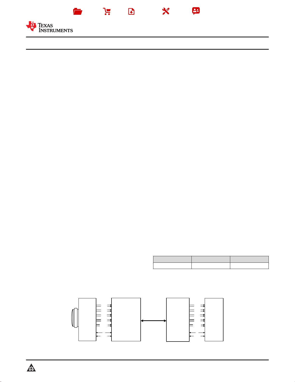
器器件件信信息息
(1)
器器件件型型号号 封封装装 封封装装尺尺寸寸((标标称称值值))
DS90UB935-Q1 VQFN (32) 5.00mm × 5.00mm
(1) 要了解所有可用封装,请见产品说明书末尾的可订购产品附
录。
典典型型应应用用


剩余93页未读,继续阅读
资源评论

 qq_335607272023-02-02#完美解决问题 #运行顺畅 #内容详尽 #全网独家 #注释完整
- m0_745259962023-02-02#完美解决问题 #运行顺畅 #内容详尽 #全网独家 #注释完整


