没有合适的资源?快使用搜索试试~ 我知道了~
TI-TLC6C5724-Q1.pdf
需积分: 13 0 下载量 90 浏览量
2022-11-16
23:50:51
上传
评论 5
收藏 1017KB PDF 举报
温馨提示
试读
57页
TI-TLC6C5724-Q1.pdf
资源推荐
资源详情
资源评论
V
CC
= 3 V - 5.5 V
LED Supply
µC
SDI
SCK
LATCH
GCLK
BLANK
SDO
ERR
VCC
SENSE
OUTG0
OUTR0
OUTB0
OUTB7
OUTR7
OUTG7
IREF
Copyright © 201 7, Texas Instrumen ts Incorpor ated
Product
Folder
Order
Now
Technical
Documents
Tools &
Software
Support &
Community
本文档旨在为方便起见,提供有关 TI 产品中文版本的信息,以确认产品的概要。 有关适用的官方英文版本的最新信息,请访问 www.ti.com,其内容始终优先。 TI 不保证翻译的准确
性和有效性。 在实际设计之前,请务必参考最新版本的英文版本。
English Data Sheet: SLASEK2
TLC6C5724-Q1
ZHCSIO0A –DECEMBER 2017–REVISED AUGUST 2018
TLC6C5724-Q1 车车用用 24 通通道道完完整整诊诊断断恒恒流流 RGB LED 驱驱动动器器
1
1 特特性性
1
• 符合面向汽车应用的 AEC-Q100 标准, 具有
– 器件温度等级 1:-40℃ 至 125℃,T
A
• 24 个恒定电流阱输出通道
– 50mA 最大输出电流
– 8V 最大输出电压
– 三个输出组:OUTRn、OUTGn、OUTBn
• 输出电流调整
– 针对每个通道提供 7 位点校正
– 针对每个组提供 8 位强度控制
• 集成 PWM 灰度发生器
– 可为每个单独通道进行 PWM 调光
– 可调节全局灰度模式:12 位、10 位和 8 位
• 保护和诊断
– LED 开路检测、LED 短路检测、输出 GND 短
路检测
– 相邻引脚短路检测
– 预热警告、热关断
– IREF 电阻器开路及短路检测和保护
– 用于 GCLK 错误检测和 LOD_LSD 寄存器错误
检查的负位切换
– LOD_LSD 电路自检
• 可编程输出压摆率
• 输出通道组延迟
• 串行数据接口
2 应应用用
• 车用仪表盘
• 车用局部调光显示屏
• 车用面板
• 车用 HVAC 控制面板
• 车用中心堆栈显示屏
• 车内 RGB 环境照明
• 车用线控换档和变速器
3 说说明明
有一些 适用于 指示灯和 LCD 局部调光背光照明的汽
车应用。对于此类 应用,,多数人认为需要使用多通
道恒定电流 LED 驱动器。要求获取相同的强度和 LED
色温。为确保系统级安全起见,LED 驱动器必须能够
检测故障。
TLC6C5724-Q1 器件是一款车用 24 通道恒定电流
RGB LED 驱动器,可利用该器件在该 LED 上进行测
试。TLC6C5724-Q1 器件可提供最高 50mA 的输出电
流(由外部电阻器设定)。该器件具有 7 位点校正功
能,每路输出 2 个范围。该器件还针对每个颜色组的
输出提供 8 位强度控制功能。可通过 12 位、10 位或
8 位灰度控制调整每个输出的强度。该器件的电路能够
检测各种系统故障,其中包括 LED 故障、邻近引脚短
路故障、基准电阻器故障等。压摆率控制具有 2 个可
调节位置,可最大限度地降低系统噪声。输出电平从一
个 LED 组变到另一个 LED 组时有一段时间间隔。此
间隔有助于减小启动电流。SDI 和 SDO 引脚允许串联
多个器件,并通过一个串行接口控制。
器器件件信信息息
(1)
器器件件型型号号 封封装装 封封装装尺尺寸寸((标标称称值值))
TLC6C5724-Q1 HTSSOP (38) 6.20mm x 12.50mm
(1) 如需了解所有可用封装,请参阅数据表末尾的可订购产品附
录。
典典型型应应用用原原理理图图
2
TLC6C5724-Q1
ZHCSIO0A –DECEMBER 2017 –REVISED AUGUST 2018
www.ti.com.cn
版权 © 2017–2018, Texas Instruments Incorporated
目目录录
1 特特性性.......................................................................... 1
2 应应用用.......................................................................... 1
3 说说明明.......................................................................... 1
4 修修订订历历史史记记录录 ........................................................... 2
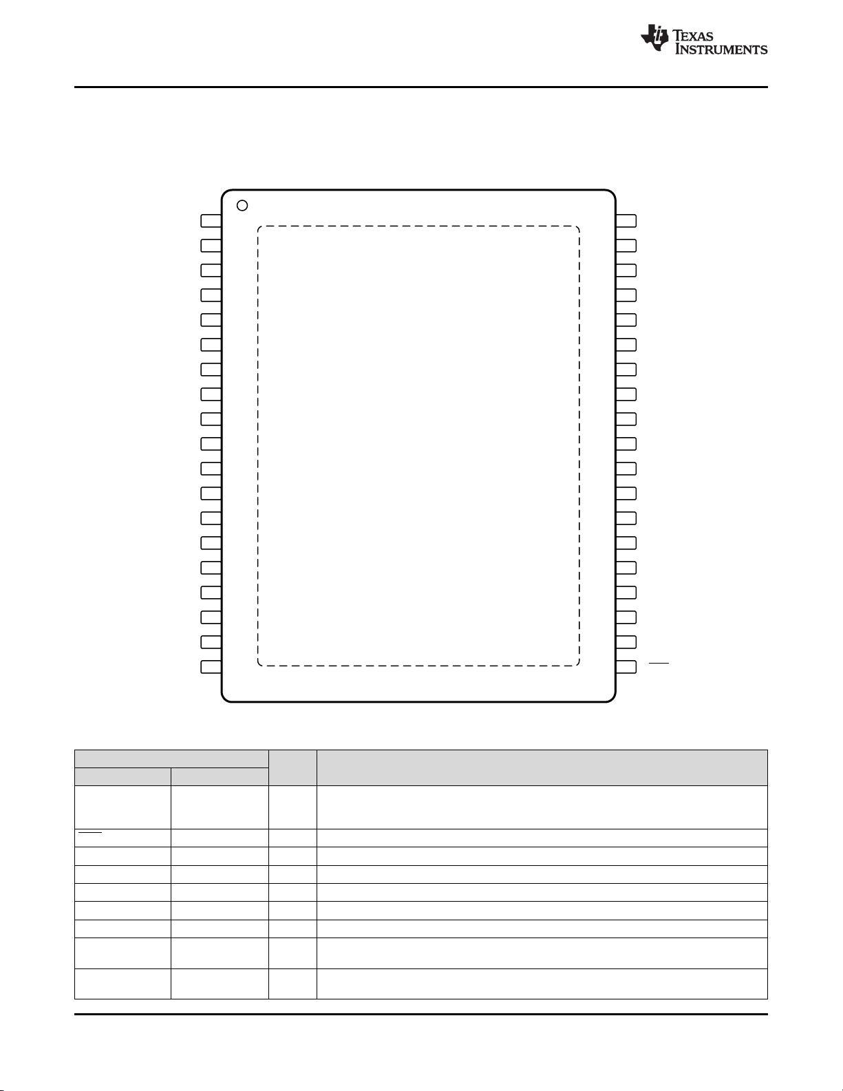
5 Pin Configuration and Functions......................... 4
6 Specifications......................................................... 6
6.1 Absolute Maximum Ratings ...................................... 6
6.2 ESD Ratings.............................................................. 6
6.3 Recommended Operating Conditions....................... 6
6.4 Thermal Information.................................................. 6
6.5 Electrical Characteristics........................................... 7
6.6 Timing Requirements................................................ 9
6.7 Switching Characteristics.......................................... 9
6.8 Typical Characteristics............................................ 21
7 Detailed Description............................................ 22
7.1 Overview ................................................................. 22
7.2 Functional Block Diagram ....................................... 22
7.3 Feature Description................................................. 23
7.4 Device Functional Modes........................................ 32
7.5 Programming .......................................................... 32
7.6 Register Maps......................................................... 39
8 Application and Implementation ........................ 49
8.1 Application Information............................................ 49
8.2 Typical Application ................................................. 49
9 Power Supply Recommendations...................... 51
10 Layout................................................................... 51
10.1 Layout Guidelines ................................................. 51
10.2 Layout Example .................................................... 51
11 器器件件和和文文档档支支持持 ..................................................... 52
11.1 接收文档更新通知 ................................................. 52
11.2 社区资源................................................................ 52
11.3 商标 ....................................................................... 52
11.4 静电放电警告......................................................... 52
11.5 术语表 ................................................................... 52
12 机机械械、、封封装装和和可可订订购购信信息息....................................... 53
4 修修订订历历史史记记录录
Changes from Original (December 2017) to Revision A Page
• 更改了数据表标题 ................................................................................................................................................................... 1
• 更改了
特性
列表中的项目 ........................................................................................................................................................ 1
• 更改了第一节 .......................................................................................................................................................................... 1
• 更改了
说明
部分中的内容 ....................................................................................................................................................... 1
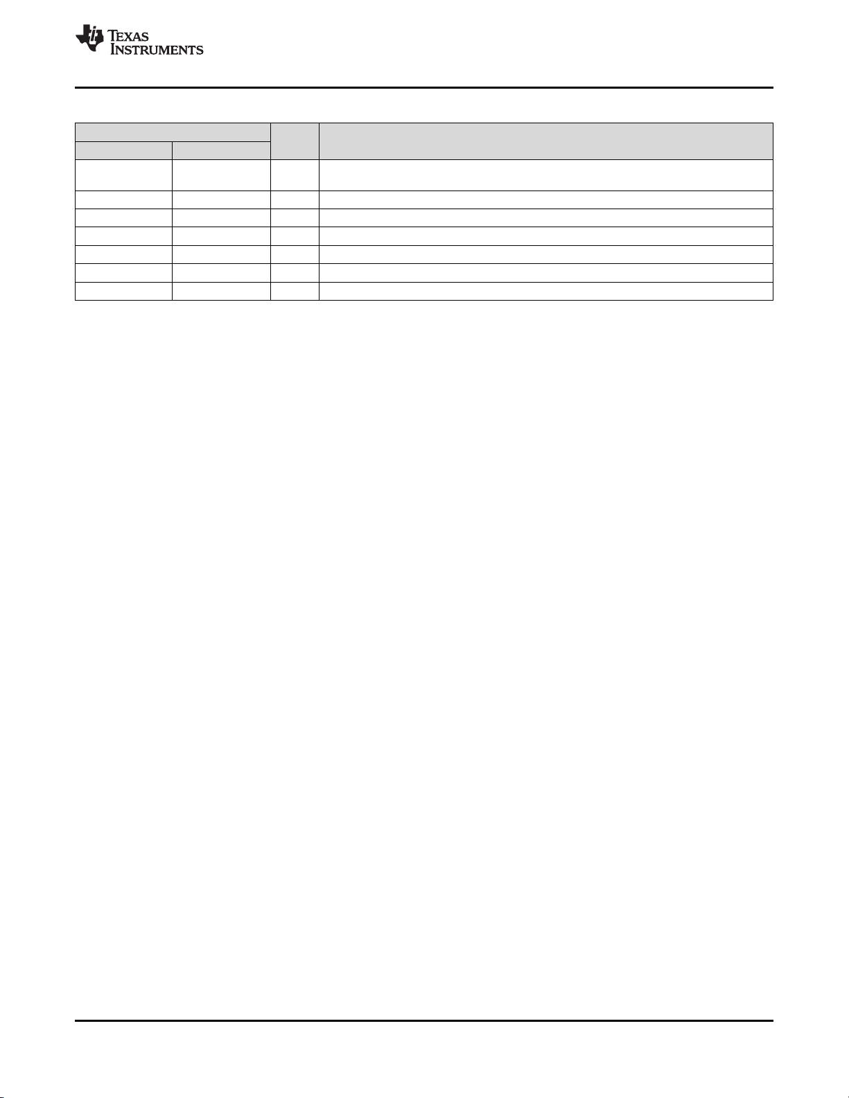
• Changed the descriptions for the GCLK, OUTBx, OUTGx, OUTRx, SENSE, and Thermal pad rows of the Pin
Functions table ...................................................................................................................................................................... 4
• Deleted a sentence and added a paraagraph at the end of the Grayscale Configuration section ...................................... 24
• Changed the section title from Display Timing Reset to PWM Auto Repeat and changed the text .................................... 25
• Changed the section title from Auto Display Repeat to PWM Timing Reset and changed the text .................................... 26
• Deleted "and PWM" from section title "LED and PWM Diagnostics" ................................................................................... 26
• Changed 表 1 ....................................................................................................................................................................... 26
• Changed the text following 表 1 .......................................................................................................................................... 26
• Changed the 表 2 dolumn headers ...................................................................................................................................... 26
• Changed the 表 3 table headers and the text following the table ........................................................................................ 26
• Changed "two kinds" to "two sets" in the sentence immediately following 表 3 .................................................................. 26
• Changed the text preceding 表 6.......................................................................................................................................... 27
• Added a table note to 表 6 .................................................................................................................................................. 28
• Deleted the first sentence following 表 6 ............................................................................................................................. 28
• Changed the text and deleted two tables in the Adjacent-Pin-Short Check section ........................................................... 28
• Added text and two tables following 表 8 ............................................................................................................................. 29
• Changed the text of the IREF Short and IREF Open Detection section .............................................................................. 29
• Changed the contents of the OUTUT column in 表 11 ....................................................................................................... 29
• Changed the text in the Pre-Thermal Warning Flag section ................................................................................................ 29
• Changed the text in the Thermal Error Flag section ............................................................................................................ 30
• Changed the text and deleted a diagram in the Negate Bit Toggle section......................................................................... 30
• Changed the text and deleted a diagram in the LOD_LSD Self-Test section ..................................................................... 30
3
TLC6C5724-Q1
www.ti.com.cn
ZHCSIO0A –DECEMBER 2017–REVISED AUGUST 2018
Copyright © 2017–2018, Texas Instruments Incorporated
修修订订历历史史记记录录 (接接下下页页)
• Changed the text in the ERROR Clear section .................................................................................................................... 31
• Changed the text in the Global Reset section...................................................................................................................... 31
• Changed the LED supply voltage from 7 V to 8 V in the Power Up section ........................................................................ 32
• Added the TEF register, where the overtemperature fault is latched................................................................................... 32
• Added a sentence to paragraph 2 of the Register Write and Read section, changed "data" to "288-bit data", and
changed "last SCK rising edge" to "288th SCK rising edge"................................................................................................ 32
• Changed "data" to "288-bit data" in the FC-BC-DC Write section ....................................................................................... 33
• Changed "sink current" to "APS current" and added "APS detection time" to the definition for bits 200 and 199,
respectively........................................................................................................................................................................... 33
• Deleted two equations preceding 表 16 .............................................................................................................................. 35
• Changed the titles of 表 16, 表 17, and 表 18 ...................................................................................................................... 35
• Added 公式 5 to calculate duty cycle.................................................................................................................................... 36
• Changed "OUTB0" to "OUTG0" for bits 167–156 in 表 19................................................................................................... 36
• Changed the last sentence of the Special Command Function section............................................................................... 37
• Changed the wording and deleted three figures in the Register Maps section ................................................................... 39
• Changed bit numbers 287 and 286 to 277 and 276 in Figure 28 ....................................................................................... 39
• Changed "Output slew rate" to "Output slew-rate time" for bit 203...................................................................................... 43
• Changed the text in the Typical Application section............................................................................................................. 49
• Added a sentence and a figure to the Detailed Design Procedure section ......................................................................... 50
• Added the Application Curves section to the data sheet...................................................................................................... 50
• Changed the LED supply voltage from 7 V to 8 V and added a sentence to the Power Supply Recommendations
section ................................................................................................................................................................................. 51
• Added positioning information for the IREF resistor to the Layout Guidelines section ........................................................ 51
1SDI 38 SENSE
2SCK 37 NC
3LATCH 36 BLANK
4GCLK 35
V
CC
5GCLK 34 IREF
6GCLK 33 GND
7OUTG0 32 OUTG7
8OUTR0 31 OUTR7
9OUTB0 30 OUTB7
10OUTG1 29 OUTG6
11OUTR1 28 OUTR6
12OUTB1 27 OUTB6
13OUTG2 26 OUTG5
14OUTR2 25 OUTR5
15OUTB2 24 OUTB5
16OUTG3 23 OUTG4
17OUTR3 22 OUTR4
18OUTB3 21 OUTB4
19SDO 20 ERR
Not to scale
Thermal
Pad
4
TLC6C5724-Q1
ZHCSIO0A –DECEMBER 2017 –REVISED AUGUST 2018
www.ti.com.cn
Copyright © 2017–2018, Texas Instruments Incorporated
5 Pin Configuration and Functions
DAP PowerPAD™ Package
38-Pin HTSSOP With Exposed Thermal Pad
Top View
Pin Functions
PIN
I/O DESCRIPTION
NAME NO.
BLANK 36 I
Blank all outputs. BLANK low forces all channels off. Grayscale counter resets, grayscale
PWM timing controller is initialized. BLANK high starts grayscale PWM timing controller,
channels are controlled by PWM timing controller.
ERR 20 O Open-drain error feedback
GCLK 4, 5, 6 I Clock input for grayscale PWM counter. The three pins are internally connected together.
GND 33 — Power ground
IREF 34 I Reference-current pin for setting the full-scale output current
LATCH 3 I Latch-enable input pin
NC 37 — No internal connection
OUTB0–OUTB7
9, 12, 15, 18, 21,
24, 27, 30
O Constant-current outputs for color group B
OUTG0–OUTG7
7, 10, 13,16, 23,
26, 29, 32
O Constant-current outputs for color group G
5
TLC6C5724-Q1
www.ti.com.cn
ZHCSIO0A –DECEMBER 2017–REVISED AUGUST 2018
Copyright © 2017–2018, Texas Instruments Incorporated
Pin Functions (continued)
PIN
I/O DESCRIPTION
NAME NO.
OUTR0–OUTR7
8, 11, 14,17, 22,
25, 28, 31
O Constant-current outputs for color group R
SCK 2 I Data-shift clock-input pin
SDI 1 I Serial data-in pin
SDO 19 O Serial data-out pin
SENSE 38 I Connect to LED supply for LED diagnostics
V
CC
35 I Power supply pin
Thermal pad — — Connect to ground to improve thermal performance
剩余56页未读,继续阅读
资源评论
不觉明了
- 粉丝: 3164
- 资源: 5429
上传资源 快速赚钱
- 我的内容管理 展开
- 我的资源 快来上传第一个资源
- 我的收益 登录查看自己的收益
- 我的积分 登录查看自己的积分
- 我的C币 登录后查看C币余额
- 我的收藏
- 我的下载
- 下载帮助
安全验证
文档复制为VIP权益,开通VIP直接复制
信息提交成功