TI-TPS92515-Q1.pdf
需积分: 12 79 浏览量
2022-11-16
23:36:27
上传
评论 5
收藏 2.24MB PDF 举报

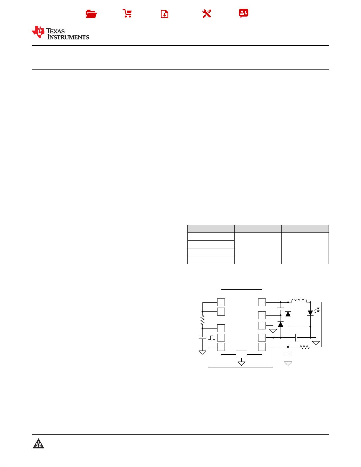
VCC
CSN
TPS92515
SW
1
2
3
4
IADJ
PWM
COFF
GND
10
9
8
7
56 DRN
VIN
BOOT
V
OUT
V
IN
PAD
Copyright © 2016, Texas Instruments Incorporated
Product
Folder
Sample &
Buy
Technical
Documents
Tools &
Software
Support &
Community
An IMPORTANT NOTICE at the end of this data sheet addresses availability, warranty, changes, use in safety-critical applications,
intellectual property matters and other important disclaimers. PRODUCTION DATA.
English Data Sheet: SLUSBZ6
TPS92515
,
TPS92515-Q1
,
TPS92515HV
,
TPS92515HV-Q1
ZHCSFD3A –APRIL 2016–REVISED AUGUST 2016
TPS92515x 集集成成有有 N 沟沟道道 FET、、
高高侧侧电电流流感感测测和和分分流流 FET PWM 调调光光功功能能的的 2A 降降压压 LED 驱驱动动器器
1
1 特特性性
1
• 符合 AEC-Q100 1 级标准
• 集成 290mΩ(典型值)内部 N 沟道场效应晶体管
(FET)
• 输入电压范围:
– TPS92515x:5.5V 至 42V
– TPS92515HVx:5.5V 至 65V
– 启动后工作电压低至 5.15V
• 低偏移高侧峰值电流比较器
• 高达 2A 的恒定平均电流
• 固有逐周期电流限制
• 多种调光方法
– 10,000:1 分流脉宽调制 (PWM) 调光范围
– 1000:1 PWM 调光范围
– 200:1 模拟调光范围
• 简单的恒定关断时间控制
– 无环路补偿
– 快速瞬态响应
• 散热增强型 HVSSOP 封装
• 集成热保护
2 应应用用
• 汽车照明:LED 开关矩阵 AFS 头灯,DRL,远光
灯/近光灯,雾灯,尾灯,转向信号灯,轮廓灯,售
后市场
• 工业照明:工厂自动化、飞行时间 (TOF)、电器、
零售照明、机器视觉检测、紧急出口和/或安全照
明、医用照明、舞台和场地照明
• 农业、航海和重工业照明
• 高对比度分流 FET 调光
3 说说明明
TPS92515 系列器件是集成了低电阻 N 沟道金属氧化
物半导体场效应晶体管 (MOSFET) 的紧凑型单片开关
稳压器。该系列器件适用于 注重 高效率、高带宽、
PWM 和/或模拟调光以及小尺寸的高亮度 LED 照明应
用。
该稳压器利用恒定关断时间和峰值电流控制功能来运
行。工作原理十分简单:在基于输出电压的一段关断时
间后,即开始导通时间。达到电感峰值电流阈值后,导
通时间立即结束。TPS92515 器件可配置为在分流
FET 调光周期的导通和关断时间内保持恒定的纹波峰
峰值。这非常适合在整个分流 FET 调光范围内保持线
性响应。
稳态精度是在低偏移高侧比较器的支持下得到保证。可
单独使用模拟或 PWM 调光技术来调制 LED 电流,也
可同时使用这两种技术来调制 LED 电流。其他 特性
包括欠压闭锁 (UVLO)、宽输入电压操作、固有 LED
开路操作和热关断功能,其工作温度范围较宽。
TPS92515 和 TPS92515-Q1 器件的工作输入电压范
围高达 42V。TPS92515HV 和 TPS92515HV-Q1 提供
输入范围高达 65V 的高电压选项。所有器件均采用散
热增强型 10 引脚 HVSSOP 封装。
器器件件信信息息
(1)
器器件件型型号号 封封装装 封封装装尺尺寸寸((标标称称值值))
TPS92515
HVSSOP (10) 3mm x 3mm
TPS92515-Q1
TPS92515HV
TPS92515HV-Q1
(1) 要了解所有可用封装,请参见数据表末尾的可订购产品附录。
简简化化的的降降压压 LED 驱驱动动器器应应用用

剩余40页未读,继续阅读
资源评论


不觉明了
- 粉丝: 3102
- 资源: 5337


