TI-TPS51200A-Q1.pdf
需积分: 10 16 浏览量
2022-11-20
17:26:20
上传
评论 5
收藏 2.07MB PDF 举报

2
3
4
5
1
9
8
7
6
10
TPS51200A-Q1
REFIN
VLDOIN
VO
PGND
VOSNS
VIN
PGOOD
GND
EN
REFOUT
3.3 V
IN
PGOOD
SLP_S3
VTTREF
VLDOIN
V
TT
V
DDQ
Product
Folder
Order
Now
Technical
Documents
Tools &
Software
Support &
Community
本文档旨在为方便起见,提供有关 TI 产品中文版本的信息,以确认产品的概要。 有关适用的官方英文版本的最新信息,请访问 www.ti.com,其内容始终优先。 TI 不保证翻译的准确
性和有效性。 在实际设计之前,请务必参考最新版本的英文版本。
English Data Sheet: SLUSD58
TPS51200A-Q1
ZHCSIL4A –JUNE 2018–REVISED DECEMBER 2018
TPS51200A-Q1 灌灌电电流流和和拉拉电电流流 DDR 终终端端稳稳压压器器
1
1 特特性性
1
• 符合面向汽车应用的 AEC-Q100 AEC-Q100 标
准:
– 器件温度等级 1:
–40°C ≤ T
A
≤ 125°C
– 器件 HBM ESD 分类等级 2
– 器件 CDM ESD 分类等级 C4B
• 扩展的可靠性测试
• 输入电压:支持 2.5V 和 3.3V 电源轨
• VLDOIN 电压范围:1.1V 至 3.5V
• 具有压降补偿功能的灌电流和拉电流终端稳压器
• 所需最小输出电容为 20μF(通常为 3 × 10μF
MLCC),用于存储器终端 应用 (DDR)
• 用于监视输出稳压的 PGOOD
• EN 输入
• REFIN 输入允许直接或通过电阻分压器灵活进行输
入跟踪
• 远程检测 (VOSNS)
• ±10mA 缓冲基准 (REFOUT)
• 内置软启动、UVLO 和 OCL
• 热关断
• 符合 DDR、DDR2 JEDEC 规范;支持 DDR3、低
功耗 DDR3 和 DDR4 VTT 应用
• 带外露散热焊盘的 VSON-10 封装
2 应应用用
• 用于 DDR、DDR2、DDR3、低功耗 DDR3 和
DDR4 的存储器终端稳压器
• 笔记本电脑、台式机、服务器
• 电信和数据通信、GSM 基站、液晶 (LCD) 电视和
等离子 (PDP) 电视、复印机和打印机、机顶盒
3 说说明明
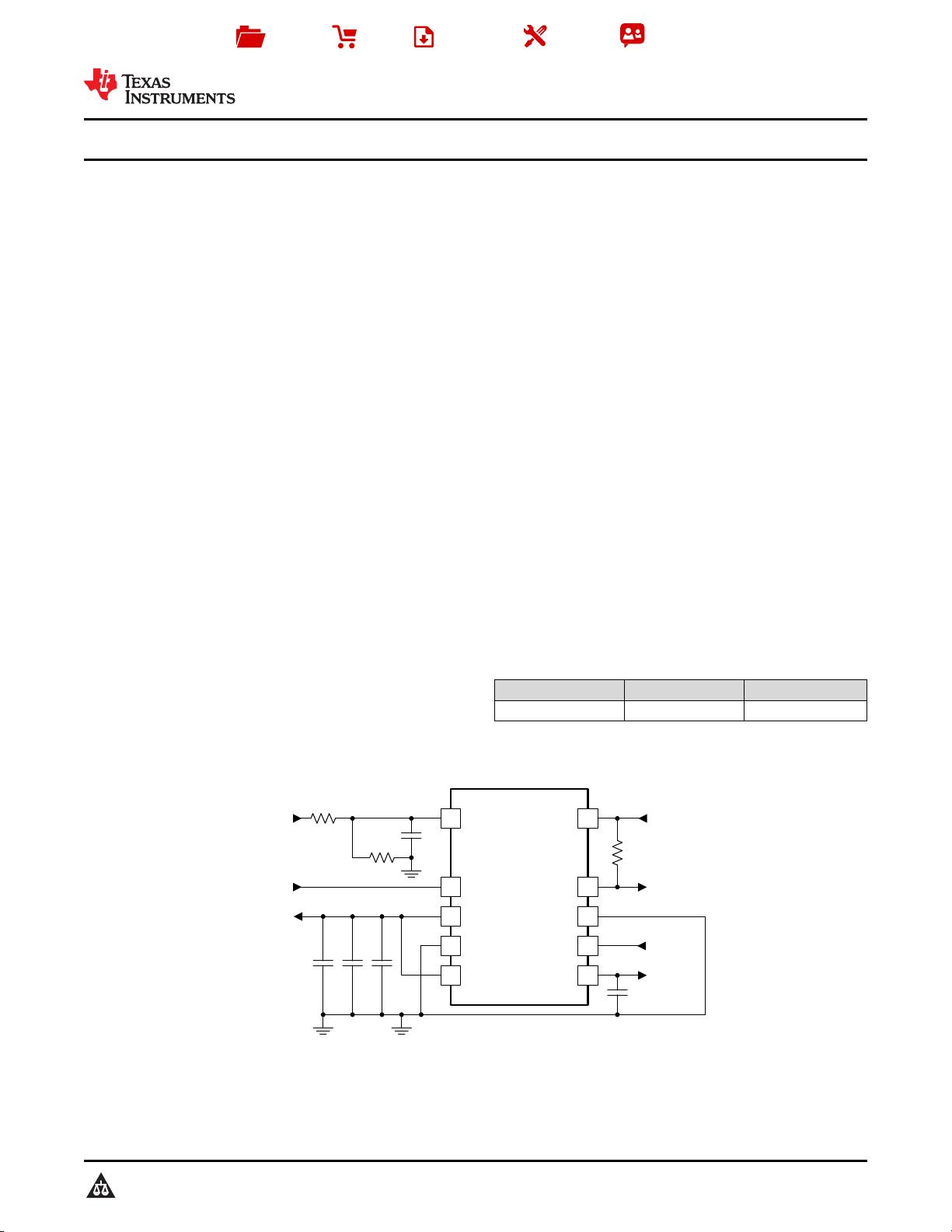
TPS51200A-Q1 器件是一款灌电流和拉电流双倍数据
速率 (DDR) 终端稳压器,专门针对低输入电压、低成
本、低噪声的空间受限型系统而设计。
此器件可保持快速的瞬态响应,最低仅需 20μF 输出电
容。此器件支持遥感功能,并且可满足 DDR、
DDR2、DDR3、低功耗 DDR3 和 DDR4 VTT 总线终
端的所有电源要求。
此外,该器件还提供一个开漏 PGOOD 信号来监测输
出稳压,并提供一个 EN 信号在 S3(挂起至 RAM)
期间针对 DDR 应用进行 VTT 放电。
此器件采用高效散热型 VSON-10 封装,具有绿色环保
和无铅的特性。该器件的额定温度范围为 –40°C 至
125°C。
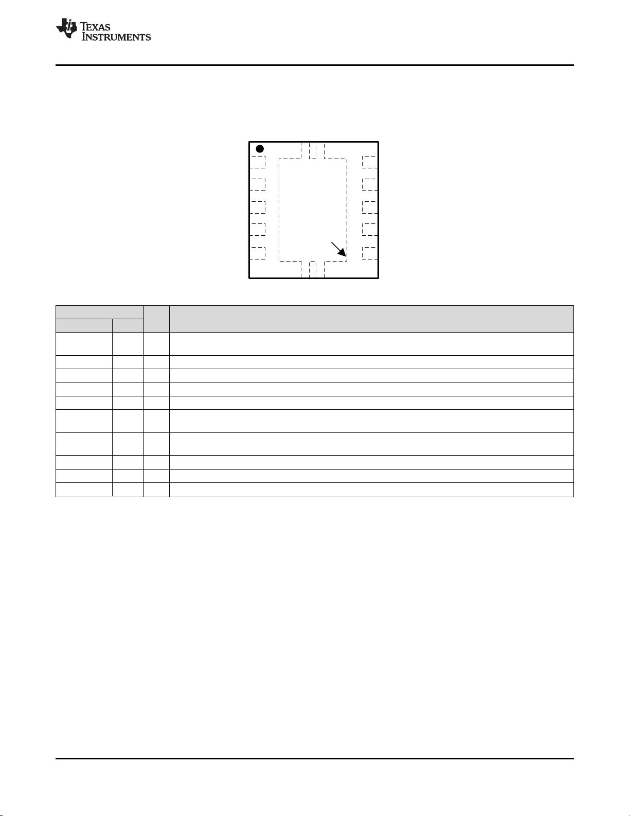
器器件件信信息息
(1)
器器件件型型号号 封封装装 封封装装尺尺寸寸((标标称称值值))
TPS51200A-Q1 VSON (10) 3.00mm × 3.00mm
(1) 如需了解所有可用封装,请见数据表末尾的可订购产品附录。
简简化化的的 DDR 应应用用

剩余38页未读,继续阅读
资源评论


