没有合适的资源?快使用搜索试试~ 我知道了~
TI-DP83TC814S-Q1.pdf
需积分: 9 1 下载量 88 浏览量
2022-12-16
21:34:24
上传
评论 4
收藏 5.07MB PDF 举报
温馨提示
试读
177页
以太网Phy收发器
资源推荐
资源详情
资源评论
DP83TC814x-Q1 100BASE-T1 Automotive Ethernet PHY
1 Features
• Open Alliance and IEEE 802.3bw 100BASE-T1
compliant
– Passes Level IV emissions with Integrated LPF
• SAE J2962-3 EMC compliant
• Configurable I/O voltages: 3.3 V, 2.5 V, and 1.8 V
• MAC interfaces: MII, RMII, RGMII and SGMII
• Optional separate voltage rail for MAC interface
pins (3.3 V, 2.5 V, 1.8 V)
• AEC-Q100 qualified for automotive applications:
– Temperature grade 1: –40°C to +125 °C
ambient operating temperature
– ±8-kV HBM ESD for pins 12 and 13
– IEC61000-4-2 ESD classification level 4 for
pins 12 and 13: ±8-kV contact discharge
• IEEE 1588 SFD support
• TSN compliant with 802.3br frame pre-emption
support
• Low active power operation: < 230 mW
• Diagnostic tool kit
– Signal quality indication (SQI)
– Time domain reflectometry (TDR)
– Electrostatic discharge sensor
– Voltage sensor
– PRBS Built-in Self-Test
– Loopbacks
• VQFN, wettable flank packaging
2 Applications
• ADAS
• Gateway and Body Control
• Telematics
3 Description
The DP83TC814-Q1 device is an IEEE 802.3bw-
compliant automotive PHYTER
™
Ethernet physical
layer transceiver which can work with Unshielded
Twisted Pair cable. It provides all physical layer
functions needed to transmit and receive data over
unshielded single twisted-pair cables. The device
provides xMII flexibility with support for standard MII,
RMII, RGMII, and SGMII MAC interfaces.The PHY
also integrates a low pass filter on the MDI side to
reduce emissions.
This device includes the Diagnostic Tool Kit, providing
an extensive list of real-time monitoring tools, debug
tools and test modes. Within the tool kit is the first
integrated electrostatic discharge (ESD) monitoring
tool. It is capable of counting ESD events on MDI
as well as providing real-time monitoring through the
use of a programmable interrupt. Additionally, the
DP83TC814S-Q1includes a pseudo random binary
sequence (PRBS) frame generation tool, which is
fully compatible with internal loopbacks, to transmit
and receive data without the use of a MAC. The
device is housed in a 6.00-mm × 6.00-mm, 36-pin
VQFN wettable flank package. This device is pin-2-
pin compatible with DP83TG720 (1000BASE-T1).
It is also form factor compatible with DP83TC811.
This would allow for a single PCB layout to be
used for DP83TC811, DP83TC812, DP83TC814, and
DP83TG720.
Device Information
PART NUMBER PACKAGE
(1)
BODY SIZE (NOM)
DP83TC814S-Q1 VQFN (36) 6.00 mm × 6.00 mm
DP83TC814R-Q1 VQFN (36) 6.00 mm × 6.00 mm
(1) For all available packages, see the orderable addendum at
the end of the data sheet.
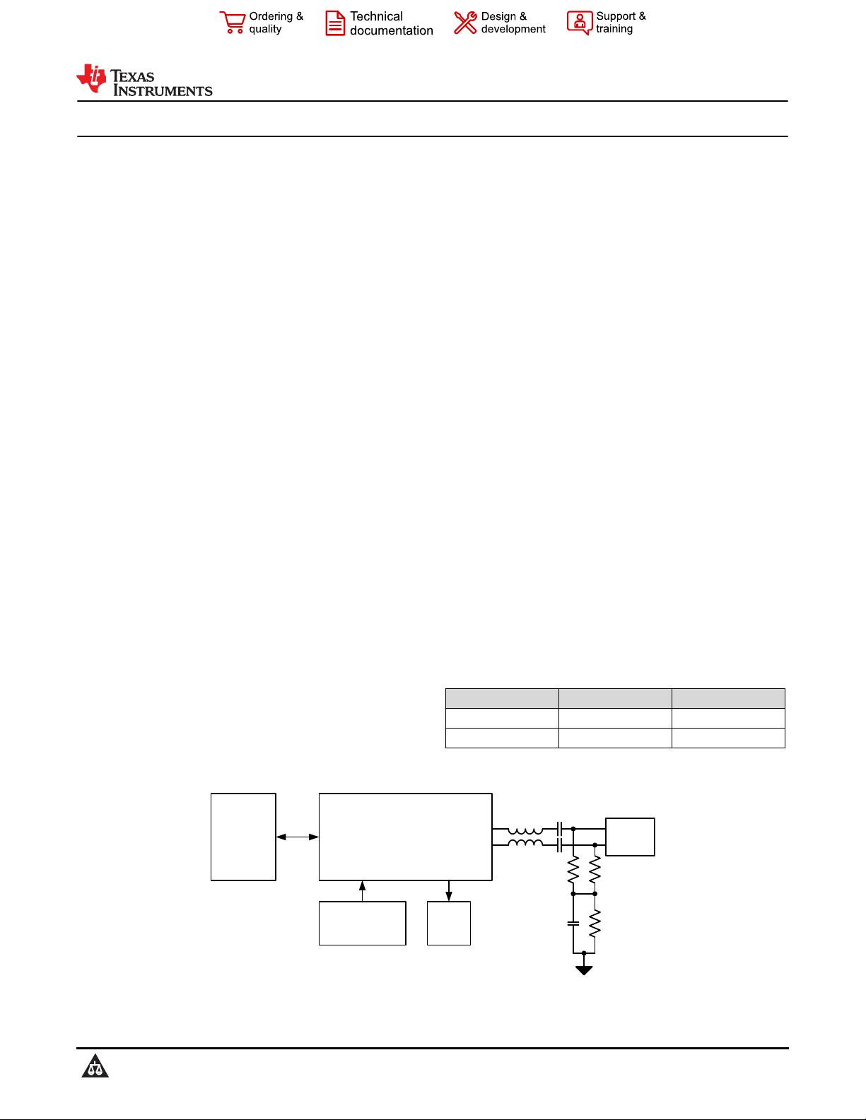
CPU/MPU
MAC
DP83TC81xS-Q1
100BASE-T1
Ethernet PHY
25MHz
Clock Source
Status
LEDs
MII
RMII
RGMII
SGMII
100BASE-T1
IEEE 802.3bw
Automotive
Connector
GND
CMC
CM
Termination
Simplified Schematic
DP83TC814S-Q1, DP83TC814R-Q1
SNLS663 – DECEMBER 2021
An IMPORTANT NOTICE at the end of this data sheet addresses availability, warranty, changes, use in safety-critical applications,
intellectual property matters and other important disclaimers. PRODUCTION DATA.
Table of Contents
1 Features............................................................................1
2 Applications..................................................................... 1
3 Description.......................................................................1
4 Revision History.............................................................. 2
5 Device Comparison Table...............................................3
6 Pin Configuration and Functions...................................4
7 Specifications................................................................ 15
7.1 Absolute Maximum Ratings...................................... 15
7.2 ESD Ratings............................................................. 15
7.3 Recommended Operating Conditions.......................15
7.4 Thermal Information..................................................16
7.5 Electrical Characteristics...........................................16
7.6 Timing Requirements................................................21
7.7 Timing Diagrams.......................................................24
7.8 Typical Characteristics.............................................. 30
8 Detailed Description......................................................32
8.1 Overview................................................................... 32
8.2 Functional Block Diagram......................................... 33
8.3 Feature Description...................................................34
8.4 Device Functional Modes..........................................43
8.5 Programming............................................................ 53
8.6 Register Maps...........................................................57
9 Application and Implementation................................ 157
9.1 Application Information........................................... 157
9.2 Typical Applications................................................ 157
10 Power Supply Recommendations............................164
11 Layout......................................................................... 166
11.1 Layout Guidelines................................................. 166
11.2 Layout Example.................................................... 168
12 Device and Documentation Support........................169
12.1 Receiving Notification of Documentation Updates169
12.2 Support Resources............................................... 169
12.3 Trademarks...........................................................169
12.4 Electrostatic Discharge Caution............................169
12.5 Glossary................................................................169
13 Mechanical, Packaging, and Orderable
Information.................................................................. 169
4 Revision History
NOTE: Page numbers for previous revisions may differ from page numbers in the current version.
DATE REVISION NOTES
December 2021 * Initial Release
DP83TC814S-Q1, DP83TC814R-Q1
SNLS663 – DECEMBER 2021
www.ti.com
2 Submit Document Feedback
Copyright © 2021 Texas Instruments Incorporated
Product Folder Links: DP83TC814S-Q1 DP83TC814R-Q1
5 Device Comparison Table
PART
NUMBER
SGMII
SUPPORT
OPERATING
TEMPERATURE
DP83TC814R-Q1 No –40°C to 125°C
DP83TC814S-Q1 Yes –40°C to 125°C
www.ti.com
DP83TC814S-Q1, DP83TC814R-Q1
SNLS663 – DECEMBER 2021
Copyright © 2021 Texas Instruments Incorporated
Submit Document Feedback
3
Product Folder Links: DP83TC814S-Q1 DP83TC814R-Q1
6 Pin Configuration and Functions
TX_EN / TX_CTRL
TX_D3
TX_D2
TX_D1/TX_P
TX_D0/TX_M
VDDIO
LED_0 / GPIO_0
MDIO
MDC
INT_N
RESET_N
DNC
XO
DNC
VDDA
TRD_P
TRD_M
RX_ER
RX_DV / CRS_DV
RX_CTRL
CLKOUT / GPIO_2
GND_ESC
DNC
NC
VDDMAC
RX_D3/RX_M
RX_D2/RX_P
RX_D1
RX_D0
RX_CLK
26 25 24 23 22 21 20 19
17
16
15
14
13
12
11
10
87654321
36
35
34
33
32
31
28
29
GND
XI
LED_1 / GPIO_1
VDDA
9
18
27
30
NC
GND_ESC
DNC
TX_CLK
Figure 6-1. DP83TC814S-Q1 RHA Package
36-Pin VQFN
DP83TC814S-Q1, DP83TC814R-Q1
SNLS663 – DECEMBER 2021
www.ti.com
4 Submit Document Feedback
Copyright © 2021 Texas Instruments Incorporated
Product Folder Links: DP83TC814S-Q1 DP83TC814R-Q1
Top View
TX_EN / TX_CTRL
TX_D3
TX_D2
TX_D1
TX_D0
VDDIO
LED_0 / GPIO_0
MDIO
MDC
INT_N
RESET_N
DNC
XO
DNC
VDDA
TRD_P
TRD_M
RX_ER
RX_DV / CRS_DV
RX_CTRL
CLKOUT / GPIO_2
GND_ESC
DNC
NC
VDDMAC
RX_D3
RX_D2
RX_D1
RX_D0
RX_CLK
26 25 24 23 22 21 20 19
17
16
15
14
13
12
11
10
87654321
36
35
34
33
32
31
28
29
GND
XI
LED_1 / GPIO_1
VDDA
9
18
27
30
NC
GND_ESC
DNC
TX_CLK
Figure 6-2. DP83TC814R-Q1 RHA Package
36-Pin VQFN
Top View
www.ti.com
DP83TC814S-Q1, DP83TC814R-Q1
SNLS663 – DECEMBER 2021
Copyright © 2021 Texas Instruments Incorporated
Submit Document Feedback
5
Product Folder Links: DP83TC814S-Q1 DP83TC814R-Q1
剩余176页未读,继续阅读
资源评论
不觉明了
- 粉丝: 3102
- 资源: 5337
上传资源 快速赚钱
- 我的内容管理 展开
- 我的资源 快来上传第一个资源
- 我的收益 登录查看自己的收益
- 我的积分 登录查看自己的积分
- 我的C币 登录后查看C币余额
- 我的收藏
- 我的下载
- 下载帮助
安全验证
文档复制为VIP权益,开通VIP直接复制
信息提交成功