没有合适的资源?快使用搜索试试~ 我知道了~
TI-DS90UR916Q-Q1.pdf
需积分: 0 0 下载量 73 浏览量
2023-02-01
23:02:45
上传
评论 4
收藏 1.07MB PDF 举报
温馨提示
试读
48页
FPD-Link解串器
资源推荐
资源详情
资源评论
DS90UR916Q
www.ti.com
SNOSB46E –MARCH 2011–REVISED APRIL 2013
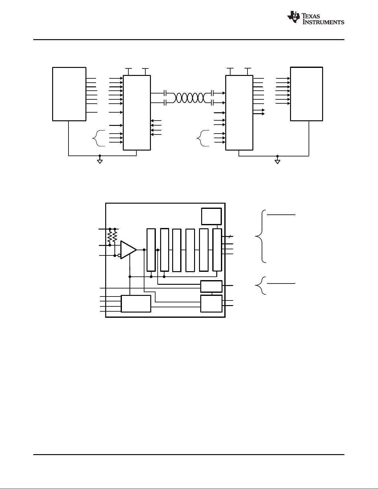
DS90UR916Q 5 - 65 MHz 24-bit Color FPD-Link II Deserializer with Image Enhancement
Check for Samples: DS90UR916Q
1
FEATURES
DESCRIPTION
The DS90UR916Q FPD-Link II deserializer operates
2
• 5 – 65 MHz PCLK support (140 Mbps – 1.82
with the DS90UR905Q FPD-Link II serializer to
Gbps)
deliver 24-bit digital video data over a single
• RGB888 + VS, HS, DE Support
differential pair. The DS90UR916Q provides features
• Image Enhancement - White Balance LUTs and
designed to enhance image quality at the display.
The high speed serial bus scheme of FPD-Link II
Adaptive Hi-FRC Dithering
greatly eases system design by eliminating skew
• AC Coupled STP Interconnect Cable up to 10
problems between clock and data, reduces the
Meters
number of connector pins, reduces the interconnect
• @ Speed Link BIST Mode and Reporting Pin
size, weight, and cost, and overall eases PCB layout.
In addition, internal DC balanced decoding is used to
• I2C Compatible Serial Control Bus
support AC-coupled interconnects.
• Power Down Mode Minimizes Power
Dissipation
The DS90UR916Q Des (deserializer) recovers the
data (RGB) and control signals and extracts the clock
• 1.8V or 3.3V Compatible LVCMOS I/O Interface
from the serial stream. The Des locks to the incoming
• Automotive Grade Product: AEC-Q100 Grade 2
serial data stream without the use of a training
Qualified
sequence or special SYNC patterns, and does not
• >8 kV HBM and ISO 10605 ESD Rating
require a reference clock. A link status (LOCK) output
signal is provided. The DS90UR916Q is ideally suited
• FAST Random Ddata Lock; No Reference
for 24-bit color applications. White balance lookup
Clock Required
tables and adaptive Hi-FRC dithering provide the user
• Adjustable Input Receiver Equalization
a cost-effective means to enhance display image
• LOCK (Real Time Link Status) Reporting Pin
quality.
• EMI Minimization on Output Parallel Bus
Serial transmission is optimized with user selectable
(SSCG)
receiver equalization. EMI is minimized by the use of
low voltage differential signaling, output slew control,
• Output Slew Control (OS)
and the Des may be configured to generate Spread
• Backward Compatible Mode for Operation with
Spectrum Clock and Data on its parallel outputs.
Older Generation Devices
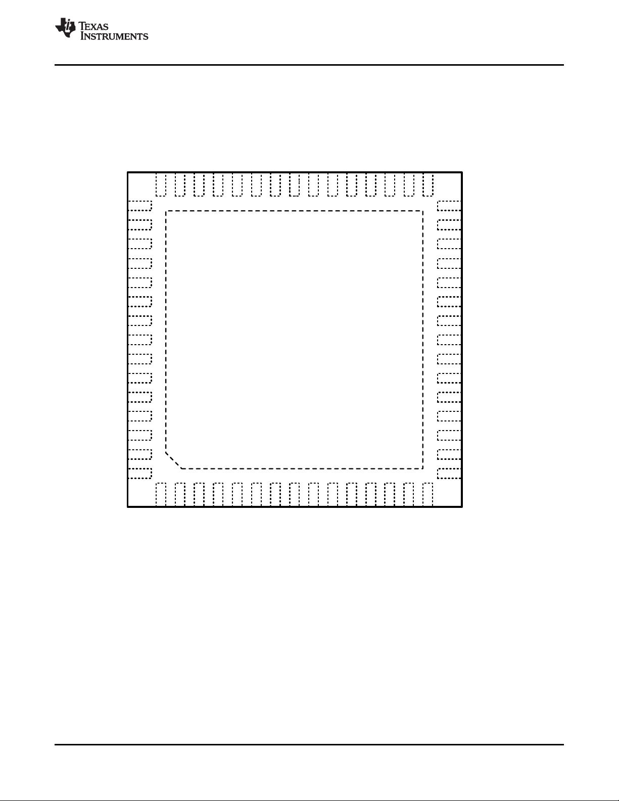
The DS90UR916Qis offered in a 60-pin WQFN
package. It is specified over the automotive AEC-
APPLICATIONS
Q100 grade 2 temperature range of -40°C to +105°C.
• Automotive Display for Navigation
• Automotive Display for Entertainment
1
Please be aware that an important notice concerning availability, standard warranty, and use in critical applications of
Texas Instruments semiconductor products and disclaimers thereto appears at the end of this data sheet.
2All trademarks are the property of their respective owners.
PRODUCTION DATA information is current as of publication date.
Copyright © 2011–2013, Texas Instruments Incorporated
Products conform to specifications per the terms of the Texas
Instruments standard warranty. Production processing does not
necessarily include testing of all parameters.
RIN-
DS90UR916Q ± DESERIALIZER
RIN+
Clock and
Data
Recovery
Timing and
Control
24
LOCK
PCLK
SSCG
Output Latch
Serial to Parallel
DC Balance Decoder
PASS
RGB [7:0]
HS
VS
DE
Error
Detector
PDB
BISTEN
CMF
SCL
SCA
ID[x]
STRAP INPUT
CONFIG [1:0]
LF_MODE
OS_PCLK/DATA
OSS_SEL
RFB
EQ [3:0]
OSC_SEL [2:0]
SSC [3:0]
MAPSEL [1:0]
STRAP INPUT
OP_LOW
FRC Dithering
1
White Balance LUT
FRC Dithering
2
R[7:0]
HS
VS
PCLK
PDB
Serializer Deserializer
DE
RGB Digital Display Interface
HOST
Graphics
Processor
FPD-Link II
1 Pair / AC Coupled
DS90UR905Q DS90UR916Q
100 ohm STP Cable
PASS
V
DDIO
PDB
SCL
SDA
CONFIG [1:0]
RFB
VODSEL
DeEmph
BISTEN
BISTEN
LOCK
ID[x]
DAP DAP
CMF
100 nF 100 nF
G[7:0]
B[7:0]
SCL
SDA
ID[x]
R[7:0]
HS
VS
PCLK
DE
G[7:0]
B[7:0]
STRAP pins
not shown
RIN+
RIN-
DOUT+
DOUT-
Optional Optional
(1.8V or 3.3V)
(1.8V or 3.3V)
1.8V
1.8V
V
DDIO
V
DDn
V
DDn
RGB Display
QVGA to XGA
24-bit or
18-bit dithered
color depth
DS90UR916Q
SNOSB46E –MARCH 2011–REVISED APRIL 2013
www.ti.com
Applications Diagram
Figure 1.
Block Diagrams
Figure 2.
2 Submit Documentation Feedback Copyright © 2011–2013, Texas Instruments Incorporated
Product Folder Links: DS90UR916Q
50
51
52
53
54
55
56
57
58
59
60
1
2
3
4
5
6
7
8
9
10
11
12
27
26
25
24
23
22
21
20
19
18
17
16
45
44
43
42
41
40
39
38
37
36
35
34
DS90UR916Q
TOP VIEW
DAP = GND
NC
PDB
VDDPR
ID[x]
CMLOUTN
CMLOUTP
RIN-
RIN+
NC
B[2]/OSS_SEL
B[0]
G[7]/EQ[3]
G[4]/EQ[0]
VDDIO
G[2]/OSC_SEL[2]
G[1]/OSC_SEL[1]
CMF
VDDCMLO
VDDR
VDDSC B[1]/RFB
G[6]/EQ[2]
G[5]/EQ[1]
G[3]
NC
SCL
B[6]/CONFIG[1]
B[4]/LF_MODE
SDA
BISTEN
VDDR
PASS/OP_LOW
R[0]/MAP_SEL[0]
R[1]/MAP_SEL[1]
R[2]
VDDIO
R[3]/SSC[0]
R[4]/SSC[1]
R[5]/SSC[2]
NC
VS
HS
B[5]/OS_PCLK
R[6]/SSC[3]
B[7]/CONFIG[0]
VDDSC
PCLK
DE
VDDIO
NC
B[3]/OS_DATA
33
32
31
R[7]
LOCK
NC
30
29
28
VDDL
NC
G[0]/OSC_SEL[0]
46
47
48
RES
NC
VDDIR
BOLD PIN NAME ± indicates I/O strap
pin associated with output pin
13
14
15
49
DS90UR916Q
www.ti.com
SNOSB46E –MARCH 2011–REVISED APRIL 2013
DS90UR916Q Pin Diagram
Figure 3. Deserializer - DS90UR916Q — Top View
Copyright © 2011–2013, Texas Instruments Incorporated Submit Documentation Feedback 3
Product Folder Links: DS90UR916Q
DS90UR916Q
SNOSB46E –MARCH 2011–REVISED APRIL 2013
www.ti.com
DS90UR916Q Deserializer Pin Descriptions
(1)
Pin Name Pin # I/O, Type Description
LVCMOS Parallel Interface
R[7:0] 33, 34, 35, I, STRAP, RED Parallel Interface Data Output Pins (MSB = 7, LSB = 0)
36, 37, 39, O, LVCMOS In power-down (PDB = 0), outputs are controlled by the OSS_SEL (See Table 5). These pins
40, 41 are inputs during power-up (See STRAP Inputs).
G[7:0] 20, 21, 22, I, STRAP, GREEN Parallel Interface Data Output Pins (MSB = 7, LSB = 0)
23, 25, 26, O, LVCMOS In power-down (PDB = 0), outputs are controlled by the OSS_SEL (See Table 5). These pins
27, 28 are inputs during power-up (See STRAP Inputs).
B[7:0] 9, 10, 11, I, STRAP, BLUE Parallel Interface Data Output Pins (MSB = 7, LSB = 0)
12, 14, 17, O, LVCMOS In power-down (PDB = 0), outputs are controlled by the OSS_SEL (See Table 5). These pins
18, 19 are inputs during power-up (See STRAP Inputs).
HS 8 O, LVCMOS Horizontal Sync Output
In power-down (PDB = 0), output is controlled by the OSS_SEL pin (See Table 5). Video
control signal pulse width must be 3 PCLKs or longer to be transmitted when the Control
Signal Filter is enabled (CONFIG[1:0] = 01). There is no restriction on the minimum transition
pulse when the Control Signal Filter is disabled (CONFIG[1:0] = 00). The signal is limited to 2
transitions per 130 PCLKs.
VS 7 O, LVCMOS Vertical Sync Output
In power-down (PDB = 0), output is controlled by the OSS_SEL pin (See Table 5). Video
control signal is limited to 1 transition per 130 PCLKs. Thus, the minimum pulse width is 130
PCLKs.
DE 6 O, LVCMOS Data Enable Output
In power-down (PDB = 0), output is controlled by the OSS_SEL pin (See Table 5). Video
control signal pulse width must be 3 PCLKs or longer to be transmitted when the Control
Signal Filter is enabled (CONFIG[1:0] = 01). There is no restriction on the minimum transition
pulse when the Control Signal Filter is disabled (CONFIG[1:0] = 00). The signal is limited to 2
transitions per 130 PCLKs.
PCLK 5 O, LVCMOS Pixel Clock Output
In power-down (PDB = 0), output is controlled by the OSS_SEL pin (See Table 5). Strobe
edge set by RFB function.
LOCK 32 O, LVCMOS LOCK Status Output
LOCK = 1, PLL is Locked, outputs are active LOCK = 0, PLL is unlocked, RGB[7:0], HS, VS,
DE and PCLK output states are controlled by OSS_SEL (See Table 5). May be used as Link
Status or to flag when Video Data is active (ON/OFF).
PASS 42 O, LVCMOS PASS Output (BIST Mode)
PASS = 1, error free transmission
PASS = 0, one or more errors were detected in the received payload
Route to test point for monitoring, or leave open if unused.
Control and Configuration — STRAP PINS
For a High State, use a 10 kΩ pull up to V
DDIO
; for a Low State, the IO includes an internal pull down. The STRAP pins are read upon
power-up and set device configuration. Pin Number listed along with shared RGB Output name in square brackets.
CONFIG[1:0] 10 [B6], STRAP Operating Modes — Pin or Register Control
9 [B7] I, LVCMOS These pins determine the DS90UR916’s operating mode and interfacing device.
w/ pull-down CONFIG[1:0] = 00: Interfacing to DS90UR905, Control Signal Filter DISABLED
CONFIG[1:0] = 01: Interfacing to DS90UR905, Control Signal Filter ENABLED
CONFIG[1:0] = 10: Interfacing to DS90UR241
CONFIG[1:0] = 11: Interfacing to DS90C241
LF_MODE 12 [B4] STRAP SSCG Low Frequency Mode — Pin or Register Control
I, LVCMOS Only required when SSCG is enabled, otherwise LF_MODE condition is a DON’T CARE (X).
w/ pull-down LF_MODE = 1, SSCG in low frequency mode (PCLK = 5-20 MHz)
LF_MODE = 0, SSCG in high frequency mode (PCLK = 20-65 MHz)
OS_PCLK 11 [B5] STRAP PCLK Output Slew Select — Pin or Register Control
I, LVCMOS OS_PCLK = 1, increased PCLK slew
w/ pull-down OS_PCLK = 0, normal (default)
OS_DATA 14 [B3] STRAP Data Output Slew Select — Pin or Register Control
I, LVCMOS OS_DATA = 1, increased DATA slew
w/ pull-down OS_DATA = 0, normal (default)
(1) 1 = HIGH, 0 = LOW.
4 Submit Documentation Feedback Copyright © 2011–2013, Texas Instruments Incorporated
Product Folder Links: DS90UR916Q
DS90UR916Q
www.ti.com
SNOSB46E –MARCH 2011–REVISED APRIL 2013
DS90UR916Q Deserializer Pin Descriptions
(1)
(continued)
Pin Name Pin # I/O, Type Description
OP_LOW 42 PASS STRAP Outputs held Low when LOCK = 1 — Pin or Register Control
I, LVCMOS NOTE: IT IS NOT RECOMMENDED TO USE ANY OTHER STRAP OPTIONS WITH THIS
w/ pull-down STRAP FUNCTION
OP_LOW = 1: all outputs are held LOW during power up until released by programming
OP_LOW release/set register HIGH
NOTE: Before the device is powered up, the outputs are in tri-state.
See Figure 23 and Figure 24.
OP_LOW = 0: all outputs toggle normally as soon as LOCK goes HIGH (default).
OSS_SEL 17 [B2] STRAP Output Sleep State Select — Pin or Register Control
I, LVCMOS NOTE: OSS_SEL STRAP CANNOT BE USED IF OP_LOW =1
w/ pull-down OSS_SEL is used in conjunction with PDB to determine the state of the outputs when
inactive. (See Table 5).
RFB 18 [B1] STRAP Pixel Clock Output Strobe Edge Select — Pin or Register Control
I, LVCMOS RFB = 1, parallel interface data and control signals are strobed on the rising clock edge.
w/ pull-down RFB = 0, parallel interface data and control signals are strobed on the falling clock edge.
EQ[3:0] 20 [G7], STRAP Receiver Input Equalization — Pin or Register Control
21 [G6], I, LVCMOS (See Table 2).
22 [G5], w/ pull-down
23 [G4]
OSC_SEL[2:0] 26 [G2], STRAP Oscillator Select — Pin or Register Control
27 [G1], I, LVCMOS (See Table 6 and Table 7).
28 [G0] w/ pull-down
SSC[3:0] 34 [R6], STRAP Spread Spectrum Clock Generation (SSCG) Range Select — Pin or Register Control
35 [R5], I, LVCMOS (See Table 3 and Table 4).
36 [R4], w/ pull-down
37 R[3]
MAP_SEL[1:0] 40 [R1], STRAP Bit Mapping Backward Compatibility / DS90UR241 Options — Pin or Register Control
41 [R0] I, LVCMOS Normal setting to b'00. See (Table 8).
w/ pull-down
Control and Configuration
PDB 59 I, LVCMOS Power Down Mode Input
w/ pull-down PDB = 1, Des is enabled (normal operation).
Refer to POWER UP REQUIREMENTS AND PDB PIN in the Applications Information
Section.
PDB = 0, Des is in power-down.
When the Des is in the power-down state, the LVCMOS output state is determined by
Table 5. Control Registers are RESET.
ID[x] 56 I, Analog Serial Control Bus Device ID Address Select — Optional
Resistor to Ground and 10 kΩ pull-up to 1.8V rail. (See Table 9).
SCL 3 I, LVCMOS Serial Control Bus Clock Input - Optional
SCL requires an external pull-up resistor to V
DDIO
.
SDA 2 I/O, LVCMOS Serial Control Bus Data Input / Output - Optional
Open Drain SDA requires an external pull-up resistor to V
DDIO
.
BISTEN 44 I, LVCMOS BIST Enable Input — Optional
w/ pull-down BISTEN = 1, BIST is enabled
BISTEN = 0, BIST is disabled
RES 47 I, LVCMOS Reserved - tie LOW
w/ pull-down
NC 1, 15, 16, Not Connected
30, 31, 45, Leave pin open (float)
46, 60
Copyright © 2011–2013, Texas Instruments Incorporated Submit Documentation Feedback 5
Product Folder Links: DS90UR916Q
剩余47页未读,继续阅读
资源评论
不觉明了
- 粉丝: 3102
- 资源: 5337
上传资源 快速赚钱
- 我的内容管理 展开
- 我的资源 快来上传第一个资源
- 我的收益 登录查看自己的收益
- 我的积分 登录查看自己的积分
- 我的C币 登录后查看C币余额
- 我的收藏
- 我的下载
- 下载帮助
安全验证
文档复制为VIP权益,开通VIP直接复制
信息提交成功