
Product
Folder
Order
Now
Technical
Documents
Tools &
Software
Support &
Community
An IMPORTANT NOTICE at the end of this data sheet addresses availability, warranty, changes, use in safety-critical applications,
intellectual property matters and other important disclaimers. PRODUCTION DATA.
English Data Sheet: SLUSCZ8
UCC27212A-Q1
ZHCSGD6 –JULY 2017
UCC27212A-Q1 汽汽车车120V 自自举举 4A 峰峰值值电电流流高高频频高高侧侧
和和低低侧侧驱驱动动器器
1
1 特特性性
1
• 符合汽车应用 要求
• 具有符合 AECA-Q100 标准的下列特性:
– 器件温度等级 –40°C 至 +140°C
– 器件 HBM 分类等级 2
– 器件 CDM 分类等级 C6
• 5V 关断欠压锁定 (UVLO)
• 通过独立输入驱动高侧和低侧配置中的两个 N 沟道
MOSFET
• 最大引导电压 120V 直流
• 4A 拉电流,4A灌电流能力
• 0.9Ω 上拉和下拉电阻
• 输入引脚能够耐受 –10V 至 +20V 的电压,并且与
电源电压范围无关
• TTL 兼容输入
• 5V 至 17V VDD 工作范围,(最大绝对值 20V)
• 7.2ns 上升时间和 5.5ns 下降时间(采用 1000pF
负载)
• 快速传播延迟时间(典型值 20ns)
• 4ns 典型延迟匹配
• 采用 SOIC8(Powerpad) 封装
2 应应用用
• 汽车应用中的 电源
• 半桥和全桥转换器
• 高电压同步降压转换器
• 双开关正向转换器
• 推挽式和有源钳位正向转换器
• D 类音频放大器
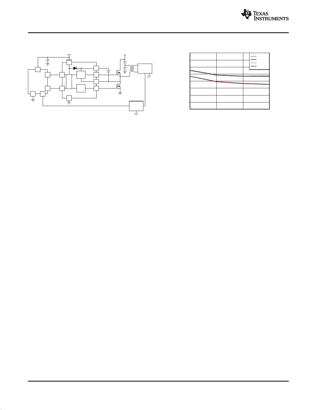
3 说说明明
UCC27212A-Q1 驱动器是基于常用的 UCC27211
MOSFET 驱动器设计的。此外,UCC27212A-Q1 具
有更宽的工作电压范围,可低至 5V,有助于降低功率
损耗。
峰值输出上拉和下拉电流分别为 4A 拉电流和 4A 灌电
流,而且上拉和下拉电阻均为 0.9Ω。这使得该器件能
够驱动大功率 MOSFET,减少由于 MOSFET 的米勒
平台导致的开关损耗。
输入结构可直接处理 -10V 电压,这提高了器件的鲁棒
性,并且无需使用整流二极管即可实现与栅极驱动变压
器直接连接。此外,输入还独立于电源电压,且具有
20V 的最大额定值。
UCC27212A-Q1 的开关节点(HS 引脚)最高可处理
-18V 电压,从而保护高侧通道不受寄生电感和杂散电
容所固有的负电压影响。UCC27212A-Q1 具有更高的
迟滞,因而支持连接至具有增强型抗噪性能的模拟或数
字 PWM 控制器。
低侧和高侧栅极驱动器是独立控制的,且彼此的开通和
关断时间均为 4ns。
由于使用了一个额定电压为 100V 的片上自举二极管,
因此无需采用外部分立式二极管。高侧和低侧驱动器均
配有欠压锁定功能,可提供对称的开通和关断行为,并
且能够在驱动电压低于额定阈值时将输出强拉至低电
平。
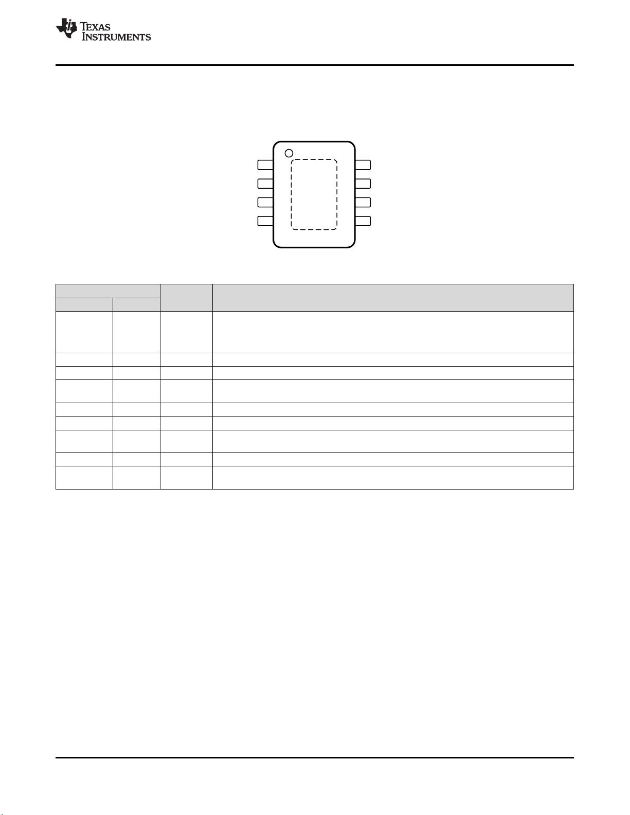
器器件件信信息息
(1)
器器件件型型号号 封封装装 封封装装尺尺寸寸((标标称称值值))
UCC27212A-Q1 SOIC8(Powerpad) 5.0mm x 6.0mm
(1) 如需了解所有可用封装,请参阅产品说明书末尾的可订购产品
附录。

剩余29页未读,继续阅读

不觉明了
- 粉丝: 4434
- 资源: 5759


最新资源
- MineAdmin是基于Hyperf框架 和 Vue3+Vite5 开发的前后端分离权限管理系统,自适应多终端 特色:后端 crud 生成 + 前端低代码 json 化配置.zip
- Preact前端框架,一键部署到云开发平台.zip
- bpi flash读ID程序
- Lessgo 是一款简单、稳定、高效、灵活的 golang web 开发框架,支持动态路由、自动化API测试文档、热编译、热更新等,实现前后端分离、系统与业务分离.zip
- 2019计算机联考408代码题
- easyink的前端服务之一,基于企业微信JS-SDK开发的企微客户端侧边栏页面.zip
- DRF-ADMIN后台管理系统项目(端代码).zip
- micro-app-chrome-plugin是基于京东零售推出的一款为micro-app框架而开发的chrome插件.zip
- front-end project template 前端快速开发模版.zip
- LaravelAdmin,简洁、直观、强悍的前端后端开发框架,让全栈开发更迅速的SPA单页面应用.LaravelAdmin,LaravelAdmin官网.zip
资源上传下载、课程学习等过程中有任何疑问或建议,欢迎提出宝贵意见哦~我们会及时处理!
点击此处反馈


评论0