没有合适的资源?快使用搜索试试~ 我知道了~
TI-UCC21530-Q1.pdf
需积分: 5 0 下载量 156 浏览量
2022-11-11
23:55:39
上传
评论 5
收藏 2.27MB PDF 举报
温馨提示
试读
46页
TI-UCC21530-Q1.pdf
资源推荐
资源详情
资源评论
UCC21530-Q1 4-A, 6-A, 5.7-kV
RMS
Isolated Dual-Channel Gate Driver
with 3.3-mm Channel-to-Channel Spacing
1 Features
• AEC-Q100 qualified with:
– Device temperature grade 1
– Device HBM ESD classification level H2
– Device CDM ESD classification level C6
• Functional Safety Quality-Managed
– Documentation available to aid functional safety
system design
• Universal: dual low-side, dual high-side or half-
bridge driver
• Wide body SOIC-14 (DWK) package
• 3.3-mm spacing between driver channels
• Switching parameters:
– 19-ns typical propagation delay
– 10-ns minimum pulse width
– 5-ns maximum delay matching
– 6-ns maximum pulse-width distortion
• Common-mode transient immunity (CMTI) greater
than 100-V/ns
• Isolation barrier life >40 years
• 4-A peak source, 6-A peak sink output
• TTL and CMOS compatible inputs
• 3-V to 18-V input VCCI range
• Up to 25-V VDD output drive supply
– 8-V and 12-V VDD UVLO options
• Programmable overlap and dead time
• Rejects input pulses and noise transients shorter
than 5 ns
• Operating temperature range –40 to +125°C
• Safety-related certifications:
– 8000-V
PK
isolation per DIN V VDE V
0884-11 :2017-01
– 5.7-kV
RMS
isolation for 1 minute per UL 1577
– CSA certification per IEC 60950-1, IEC
62368-1, IEC 61010-1 and IEC 60601-1 end
equipment standards
– CQC certification per GB4943.1-2011
2 Applications
• HEV and BEV battery chargers
• Solar string and central inverters
• AC-to-DC and DC-to-DC charging piles
• AC inverter and servo drive
• AC-to-DC and DC-to-DC power delivery
• Energy storage systems
3 Description
The UCC21530-Q1 is an isolated dual-channel gate
driver with 4-A source and 6-A sink peak current. It
is designed to drive IGBTs, Si MOSFETs, and SiC
MOSFETs up to 5-MHz with best-in-class propagation
delay and pulse-width distortion.
The input side is isolated from the two output
drivers by a 5.7-kV
RMS
reinforced isolation barrier,
with a minimum of 100-V/ns common-mode transient
immunity (CMTI). Internal functional isolation between
the two secondary-side drivers allows a working
voltage of up to 1850 V.
This driver can be configured as two low-side drivers,
two high-side drivers, or a half-bridge driver with
programmable dead time (DT). The EN pin pulled low
shuts down both outputs simultaneously and allows
for normal operation when left open or pulled high. As
a fail-safe measure, primary-side logic failures force
both outputs low.
The device accepts VDD supply voltages up to 25 V.
A wide input VCCI range from 3 V to 18 V makes
the driver suitable for interfacing with both analog and
digital controllers. All the supply voltage pins have
under voltage lock-out (UVLO) protection.
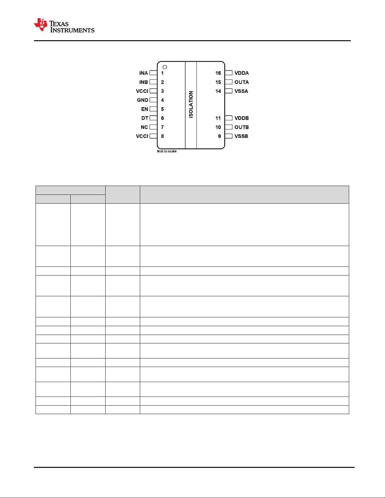
Device Information
(1)
PART NUMBER PACKAGE BODY SIZE (NOM)
UCC21530-Q1 DWK SOIC (14) 10.30 mm × 7.50 mm
UCC21530B-Q1 DWK SOIC (14) 10.30 mm × 7.50 mm
(1) For all available packages, see the orderable addendum at
the end of the data sheet.
Functional Block Diagram
www.ti.com
UCC21530-Q1
SLUSDG3D – AUGUST 2018 – REVISED APRIL 2021
Copyright © 2021 Texas Instruments Incorporated
Submit Document Feedback
1
Product Folder Links: UCC21530-Q1
UCC21530-Q1
SLUSDG3D – AUGUST 2018 – REVISED APRIL 2021
An IMPORTANT NOTICE at the end of this data sheet addresses availability, warranty, changes, use in safety-critical applications,
intellectual property matters and other important disclaimers. PRODUCTION DATA.
Table of Contents
1 Features............................................................................1
2 Applications..................................................................... 1
3 Description.......................................................................1
4 Revision History.............................................................. 2
5 Pin Configuration and Functions...................................3
Pin Functions.................................................................... 3
6 Specifications.................................................................. 4
6.1 Absolute Maximum Ratings........................................ 4
6.2 ESD Ratings............................................................... 4
6.3 Recommended Operating Conditions.........................4
6.4 Thermal Information....................................................5
6.5 Power Ratings.............................................................5
6.6 Insulation Specifications............................................. 6
6.7 Safety-Related Certifications...................................... 7
6.8 Safety-Limiting Values................................................ 7
6.9 Electrical Characteristics.............................................8
6.10 Switching Characteristics..........................................9
6.11 Insulation Characteristics Curves............................10
6.12 Typical Characteristics............................................ 11
7 Parameter Measurement Information.......................... 16
7.1 Propagation Delay and Pulse Width Distortion......... 16
7.2 Rising and Falling Time.............................................16
7.3 Input and Enable Response Time.............................16
7.4 Programable Dead Time...........................................17
7.5 Power-Up UVLO Delay to OUTPUT......................... 17
7.6 CMTI Testing.............................................................18
8 Detailed Description......................................................19
8.1 Overview................................................................... 19
8.2 Functional Block Diagram......................................... 19
8.3 Feature Description...................................................20
8.4 Device Functional Modes..........................................23
9 Layout.............................................................................37
9.1 Layout Guidelines..................................................... 37
9.2 Layout Example........................................................ 38
10 Device and Documentation Support..........................40
10.1 Documentation Support.......................................... 40
10.2 Receiving Notification of Documentation Updates..40
10.3 Community Resources............................................40
10.4 Trademarks.............................................................40
4 Revision History
NOTE: Page numbers for previous revisions may differ from page numbers in the current version.
Changes from Revision B (November 2018) to Revision C (March 2019) Page
• Initial release.......................................................................................................................................................1
Changes from Revision C (March 2019) to Revision D (April 2021) Page
• Added 8-V UVLO option to features, description, and device information sections .......................................... 1
• Added information to pin 7 in Pin function table................................................................................................. 3
• Added VDE certification, CSA master contract, and CQC certificate numbers to Safety-Related Certifications
table ................................................................................................................................................................... 7
• Added 8-V UVLO thresholds to EC table ...........................................................................................................8
• Added 8-V UVLO thresholds and hysteresis across temperature ................................................................... 11
UCC21530-Q1
SLUSDG3D – AUGUST 2018 – REVISED APRIL 2021
www.ti.com
2 Submit Document Feedback
Copyright © 2021 Texas Instruments Incorporated
Product Folder Links: UCC21530-Q1
5 Pin Configuration and Functions
Figure 5-1. DWK Package 14-Pin SOIC Top View
Pin Functions
PIN
I/O
(1)
DESCRIPTION
NAME NO.
DT 6 I
DT pin configuration:
• Tying DT to VCCI disables the DT feature and allows the outputs to overlap.
• Placing a resistor (R
DT
) between DT and GND adjusts dead time according to the
equation: DT (in ns) = 10 × R
DT
(in kΩ). TI recommends bypassing this pin with a
ceramic capacitor, 2.2 nF or greater, close to DT pin to achieve better noise immunity.
EN 5 I
Enable both driver outputs if asserted high, disable the output if set low. It is recommended
to tie this pin to VCCI if not used to achieve better noise immunity. Bypass using a ≈ 1-nF
low ESR/ESL capacitor close to EN pin when connecting to a micro controller with distance.
GND 4 P Primary-side ground reference. All signals in the primary side are referenced to this ground.
INA 1 I
Input signal for A channel. INA input has a TTL/CMOS compatible input threshold. This pin
is pulled low internally if left open. It is recommended to tie this pin to ground if not used to
achieve better noise immunity.
INB 2 I
Input signal for B channel. INB input has a TTL/CMOS compatible input threshold. This pin
is pulled low internally if left open. It is recommended to tie this pin to ground if not used to
achieve better noise immunity.
NC 7 – No internal connection. This pin can be left floating, tied to VCCI, or tied to GND.
OUTA 15 O Output of driver A. Connect to the gate of the A channel FET or IGBT.
OUTB 10 O Output of driver B. Connect to the gate of the B channel FET or IGBT.
VCCI 3 P
Primary-side supply voltage. Locally decoupled to GND using a low ESR/ESL capacitor
located as close to the device as possible.
VCCI 8 P Primary-side supply voltage. This pin is internally shorted to pin 3.
VDDA 16 P
Secondary-side power for driver A. Locally decoupled to VSSA using a low ESR/ESL
capacitor located as close to the device as possible.
VDDB 11 P
Secondary-side power for driver B. Locally decoupled to VSSB using low ESR/ESL
capacitor located as close to the device as possible.
VSSA 14 P Ground for secondary-side driver A. Ground reference for secondary side A channel.
VSSB 9 P Ground for secondary-side driver B. Ground reference for secondary side B channel.
(1) P =Power, I= Input, O= Output
www.ti.com
UCC21530-Q1
SLUSDG3D – AUGUST 2018 – REVISED APRIL 2021
Copyright © 2021 Texas Instruments Incorporated
Submit Document Feedback
3
Product Folder Links: UCC21530-Q1
6 Specifications
6.1 Absolute Maximum Ratings
Over operating free-air temperature range (unless otherwise noted)
(1)
MIN MAX UNIT
Input bias pin supply voltage VCCI to GND –0.5 20 V
Driver bias supply VDDA-VSSA, VDDB-VSSB –0.5 30 V
Output signal voltage
OUTA to VSSA, OUTB to VSSB –0.5
V
VDDA
+0.5,
V
VDDB
+0.5
V
OUTA to VSSA, OUTB to VSSB,
Transient for 200 ns
–2
V
VDDA
+0.5,
V
VDDB
+0.5
V
Input signal voltage
INA, INB, EN, DT to GND –0.5 V
VCCI
+0.5 V
INA, INB Transient for 200ns –2 V
VCCI
+0.5 V
Channel to channel internal isolation voltage |VSSA-VSSB| 1850 V
Junction temperature, T
J
(2)
–40 150 °C
Storage temperature, T
stg
–65 150 °C
(1) Stresses beyond those listed under Absolute Maximum Ratings may cause permanent damage to the device. These are stress
ratings only, which do not imply functional operation of the device at these or any other conditions beyond those indicated under
Recommended Operating Conditions. Exposure to absolute-maximum-rated conditions for extended periods may affect device
reliability.
(2) To maintain the recommended operating conditions for T
J
, see the Section 6.4.
6.2 ESD Ratings
VALUE
UNIT
V
(ESD)
Electrostatic discharge
Human-body model (HBM), per AEC Q100-002
(1)
±4000
V
Charged-device model (CDM), per AEC Q100-011 ±1500
(1) AEC Q100-002 indicates that HBM stressing shall be in accordance with the ANSI/ESDA/JEDEC JS-001 specification.
6.3 Recommended Operating Conditions
Over operating free-air temperature range (unless otherwise noted)
MIN MAX UNIT
VCCI VCCI Input supply voltage 3 18 V
VDDA-
VSSA,
VDDB-
VSSB
Driver output bias supply refer to Vss
8-V UVLO version -
UCC21530B-Q1
9.2 25 V
12-V UVLO version -
UCC21530-Q1
14.7 25 V
T
A
Ambient Temperature –40 125 °C
T
J
Junction Temperature –40 130 °C
UCC21530-Q1
SLUSDG3D – AUGUST 2018 – REVISED APRIL 2021
www.ti.com
4 Submit Document Feedback
Copyright © 2021 Texas Instruments Incorporated
Product Folder Links: UCC21530-Q1
6.4 Thermal Information
THERMAL METRIC
(1)
UCC21530-Q1
UNIT
DWK-14 (SOIC)
R
θJA
Junction-to-ambient thermal resistance 68.3 °C/W
R
θJC(top)
Junction-to-case (top) thermal resistance 31.7 °C/W
R
θJB
Junction-to-board thermal resistance 27.6 °C/W
ψ
JT
Junction-to-top characterization parameter 17.7 °C/W
ψ
JB
Junction-to-board characterization parameter 27 °C/W
(1) For more information about traditional and new thermal metrics, see the Semiconductor and IC Package Thermal Metrics application
report.
6.5 Power Ratings
VALUE UNIT
P
D
Power dissipation by UCC21530-Q1
VCCI = 18 V, VDDA/B = 15 V, INA/B = 3.3 V,
3.9 MHz 50% duty cycle square wave 1-nF
load
1810 mW
P
DI
Power dissipation by transmitter side of
UCC21530-Q1
50 mW
P
DA
, P
DB
Power dissipation by each driver side of
UCC21530-Q1
880 mW
www.ti.com
UCC21530-Q1
SLUSDG3D – AUGUST 2018 – REVISED APRIL 2021
Copyright © 2021 Texas Instruments Incorporated
Submit Document Feedback
5
Product Folder Links: UCC21530-Q1
剩余45页未读,继续阅读
资源评论
不觉明了
- 粉丝: 3137
- 资源: 5382
上传资源 快速赚钱
- 我的内容管理 展开
- 我的资源 快来上传第一个资源
- 我的收益 登录查看自己的收益
- 我的积分 登录查看自己的积分
- 我的C币 登录后查看C币余额
- 我的收藏
- 我的下载
- 下载帮助
最新资源
- 基于OpenCV的案例:图像边缘、角点和轮廓检测,图像分割,图像增强;图片拼接;运动目标检测,颜色直方图比较,三帧帧差法,抠图
- SmartPlug-html大一笔记
- SmartPlug-proteusdemo
- Preliminary Findings on Handmade Rattan Baby Crib andBassinet Designs Regarding.zip
- aveebfq_v1.2.83_downyi.com.apk
- 基于有机发光二极管(OLED)的建模优化算法的matlab仿真源码+数据+文档说明+项目说明(高分课程设计)
- hash01-test.c 本人哈希表(一)的示例代码,仅供参考!
- 处理数据.py
- 软件实施计划表.xls
- 软件开发应用软件项目提交文档目录要求(全过程)(推荐文档).xls
资源上传下载、课程学习等过程中有任何疑问或建议,欢迎提出宝贵意见哦~我们会及时处理!
点击此处反馈
安全验证
文档复制为VIP权益,开通VIP直接复制
信息提交成功