4
DS90UH949A-Q1
ZHCSIO8 –AUGUST 2018
www.ti.com.cn
Copyright © 2018, Texas Instruments Incorporated
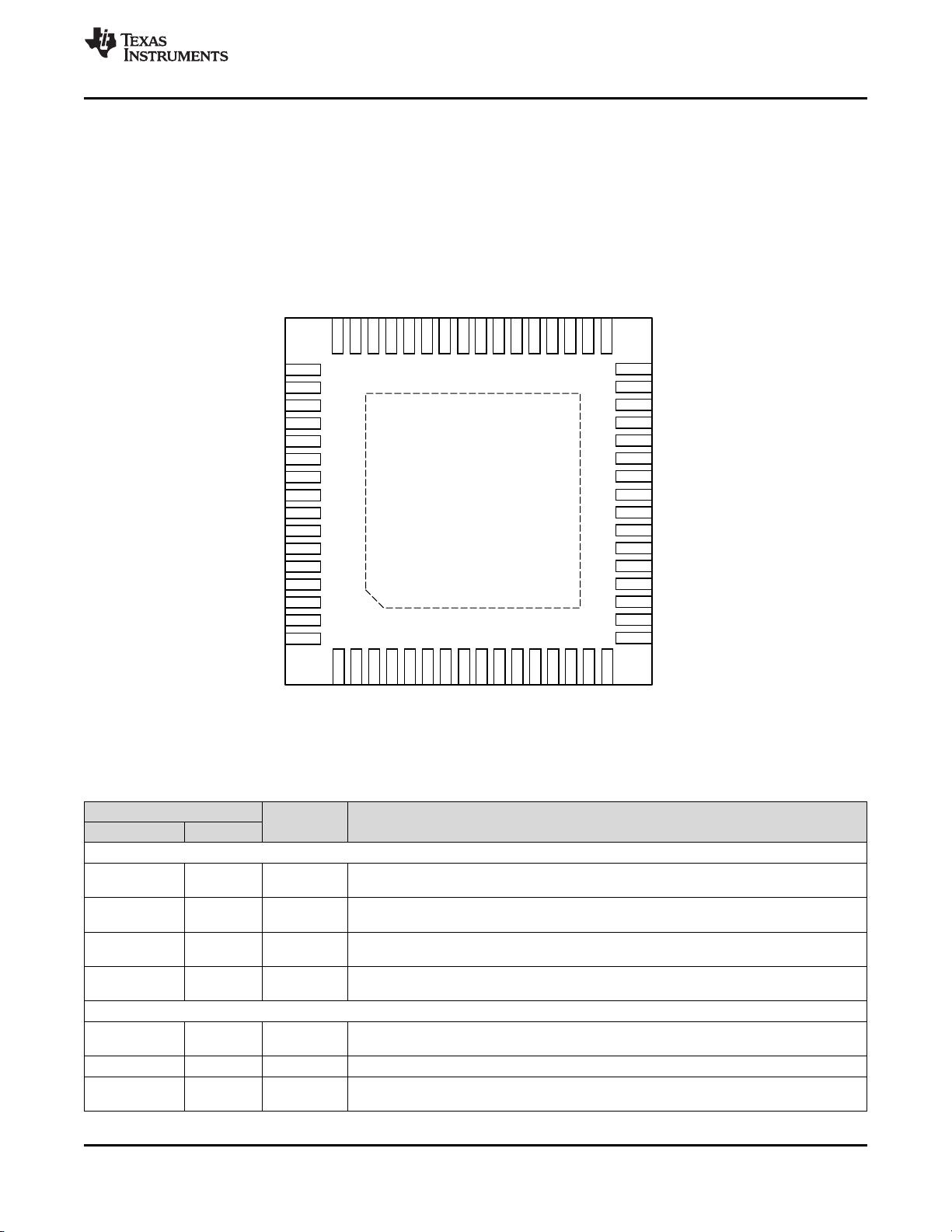
Pin Functions (continued)
PIN
I/O, TYPE DESCRIPTION
NAME NO.
DDC_SCL 45 I, Open-Drain DDC Slave Serial Clock
Pull up to RX_5V with a 47-kΩ resistor
CEC 1 IO, Open-
Drain
Consumer Electronic Control Channel Input/Output Interface.
Pullup with a 27-kΩ resistor to 3.3 V
X1 39 I, LVCMOS Optional Oscillator Input: This pin is the optional reference clock for CEC. It must be
connected to a 25 MHz 0.1% (1000ppm), 45-55% duty cycle clock source at CMOS-level
1.8 V. Leave it open if unused.
FPD-LINK III SERIAL
DOUT0- 26 O FPD-Link III Inverting Output 0
The output must be AC-coupled with a 0.1-μF capacitor for interfacing with 92x deserializers
and 0.1-μF or 33-nF capacitor for 94x deserializers
DOUT0+ 27 O FPD-Link III True Output 0
The output must be AC-coupled with a 0.1-µF capacitor for interfacing with 92x deserializers
and 0.1-μF or 33-nF capacitor for 94x deserializers
DOUT1- 22 O FPD-Link III Inverting Output 1
The output must be AC-coupled with a 0.1-µF capacitor for interfacing with 92x deserializers
and 0.1-μF or 33-nF capacitor for 94x deserializers
DOUT1+ 23 O FPD-Link III True Output 1
The output must be AC-coupled with a 0.1-µF capacitor for interfacing with 92x deserializers
and 0.1-μF or 33-nF capacitor for 94x deserializers
LFT 20 Analog FPD-Link III Loop Filter
Connect to a 10-nF capacitor to GND
CONTROL
SDA 14 IO, Open-
Drain
I2C Data Input / Output Interface
Open-drain. Must have an external pullup to resistor to 1.8 V or 3.3 V. See I2CSEL pin. DO
NOT FLOAT.
Recommended pullup: 4.7 kΩ.
SCL 15 IO, Open-
Drain
I2C Clock Input / Output Interface
Open-drain. Must have an external pullup resistor to 1.8 V or 3.3 V. See I2CSEL pin. DO
NOT FLOAT.
Recommended pullup: 4.7 kΩ.
I2CSEL 6 I, LVCMOS I2C Voltage Level Strap Option
Tie to V
DDIO
with a 10-kΩ resistor for 1.8-V I2C operation.
Leave floating for 3.3-V I2C operation.
This pin is read as an input at power up.
IDx 19 Analog I2C Serial Control Bus Device ID Address Select
MODE_SEL0 18 Analog Mode Select 0. See 表 6.
MODE_SEL1 32 Analog Mode Select 1. See 表 6.
PDB 31 I, LVCMOS Power-Down Mode Input Pin
INTB 13 O, Open-
Drain
Open-Drain. Remote interrupt. Active LOW.
Pull up to VDDIO with a 4.7-kΩ resistor.
REM_INTB 40 O, Open-
Drain
Remote interrupt. Mirrors status of INTB_IN from the deserializer.
Note: External pull-up to 1.8 V required. Recommended pullup: 4.7 kΩ.
INTB = H, Normal Operation
INTB = L, Interrupt Request
SPI PINS (DUAL LINK MODE ONLY)
MOSI 8 IO, LVCMOS SPI Master Out Slave In. Shared with D_GPIO0
MISO 10 IO, LVCMOS SPI Master In Slave Out. Shared with D_GPIO1
SPLK 11 IO, LVCMOS SPI Clock. Shared with D_GPIO2
SS 12 IO, LVCMOS SPI Slave Select. Shared with D_GPIO3
HIGH-SPEED (HS) BIDIRECTIONAL CONTROL CHANNEL GPIO PINS (DUAL LINK MODE ONLY)
D_GPIO0 8 IO, LVCMOS HS GPIO0. Shared with MOSI
D_GPIO1 10 IO, LVCMOS HS GPIO1. Shared with MISO
D_GPIO2 11 IO, LVCMOS HS GPIO2. Shared with SPLK


 我的内容管理
展开
 我的资源
快来上传第一个资源
 我的收益 登录查看自己的收益
 我的积分
登录查看自己的积分
 我的C币
登录后查看C币余额
 我的收藏
我的收藏  我的下载
我的下载  下载帮助
下载帮助 
 前往需求广场,查看用户热搜

 信息提交成功