没有合适的资源?快使用搜索试试~ 我知道了~
TI-TLC6C598-Q1.pdf
需积分: 9 0 下载量 4 浏览量
2022-11-16
23:50:03
上传
评论 5
收藏 642KB PDF 举报
温馨提示
试读
25页
TI-TLC6C598-Q1.pdf
资源推荐
资源详情
资源评论
30 mA30 mA
4/3
8-Bit Shift Register
LED Driver
MCU Serial I/F
Battery 9 V–40 V
Product
Folder
Sample &
Buy
Technical
Documents
Tools &
Software
Support &
Community
An IMPORTANT NOTICE at the end of this data sheet addresses availability, warranty, changes, use in safety-critical applications,
intellectual property matters and other important disclaimers. PRODUCTION DATA.
TLC6C598-Q1
SLIS142D –DECEMBER 2012–REVISED SEPTEMBER 2016
TLC6C598-Q1 Power Logic 8-Bit Shift Register LED Driver
1
1 Features
1
• Qualified for Automotive Applications
• AEC-Q100 Qualified With the Following Results:
– Device Temperature Grade 1: –40°C to 125°C
Ambient Operating Temperature Range
– Device HBM ESD Classification Level H2
– Device CDM ESD Classification Level C3B
• Wide Vcc From 3 V to 5.5 V
• Output Maximum Rating of.40 V
• Eight Power DMOS Transistor Outputs of 50-mA
Continuous Current With V
CC
= 5 V
• Thermal Shutdown Protection
• Enhanced Cascading for Multiple Stages
• All Registers Cleared With Single Input
• Low Power Consumption
• Slow Switching Time (t
r
and t
f
), Which Helps
Significantly With Reducing EMI
• 16-Pin TSSOP-PW Package
• 16-Pin SOIC-D Package
2 Applications
• Instrumentation Cluster
• Tell-Tale Lamps
• LED Illumination and Control
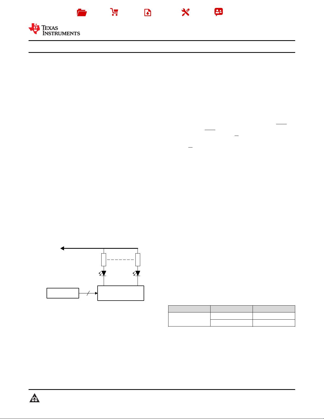
Typical Application Schematic
3 Description
The TLC6C598-Q1 is a monolithic, medium-voltage,
low-current power 8-bit shift register designed for use
in systems that require relatively moderate load
power, such as LEDs.
This device contains an 8-bit serial-in, parallel-out
shift register that feeds an 8-bit D-type storage
register. Data transfers through both the shift and
storage registers on the rising edge of the shift-
register clock (SRCK) and the register clock (RCK),
respectively. The storage register transfers data to
the output buffer when shift register clear (CLR) is
high. A low on CLR clears all registers in the device.
Holding the output enable (G) high, holds all data in
the output buffers low, and all drain outputs are off.
Holding G low makes data from the storage register
transparent to the output buffers. When data in the
output buffers is low, the DMOS transistor outputs are
off. When data is high, the DMOS transistor outputs
have sink-current capability. The serial output (SER
OUT) clocks out of the device on the falling edge of
SRCK to provide additional hold time for cascaded
applications. This provides improved performance for
applications where clock signals may be skewed,
devices are not located near one another, or the
system must tolerate electromagnetic interference.
The device contains built-in thermal shutdown
protection.
Outputs are low-side, open-drain DMOS transistors
with output ratings of 40 V and 50 mA continuous
sink-current capabilities when Vcc = 5 V. The current
limit decreases as the junction temperature increases
for additional device protection. The device also
provides up to 2000 V of ESD protection when tested
using the human-body model and 200 V when using
the machine model.
The TLC6C598-Q1 characterization is for for
operation over the operating ambient temperature
range of −40°C to 125°C.
Device Information
(1)
PART NUMBER PACKAGE BODY SIZE (NOM)
TLC6C598-Q1
SOIC (16) 9.90 mm x 3.91 mm
TSSOP (16) 5.00 mm x 4.40 mm
(1) For all available packages, see the orderable addendum at
the end of the datasheet.
2
TLC6C598-Q1
SLIS142D –DECEMBER 2012–REVISED SEPTEMBER 2016
www.ti.com
Product Folder Links: TLC6C598-Q1
Submit Documentation Feedback Copyright © 2012–2016, Texas Instruments Incorporated
Table of Contents
1 Features.................................................................. 1
2 Applications ........................................................... 1
3 Description ............................................................. 1
4 Revision History..................................................... 2
5 Pin Configuration and Functions......................... 3
6 Specifications......................................................... 4
6.1 Absolute Maximum Ratings ...................................... 4
6.2 ESD Ratings.............................................................. 4
6.3 Recommended Operating Conditions....................... 4
6.4 Thermal Information.................................................. 4
6.5 Electrical Characteristics........................................... 5
6.6 Timing Requirements................................................ 5
6.7 Switching Characteristics.......................................... 6
6.8 Timing Waveforms .................................................... 7
6.9 Typical Characteristics.............................................. 8
7 Parameter Measurement Information .................. 9
8 Detailed Description............................................ 11
8.1 Overview ................................................................. 11
8.2 Functional Block Diagram ....................................... 11
8.3 Feature Description................................................. 12
8.4 Device Functional Modes........................................ 12
9 Application and Implementation ........................ 13
9.1 Application Information............................................ 13
9.2 Typical Application ................................................. 13
10 Power Supply Recommendations ..................... 16
11 Layout................................................................... 16
11.1 Layout Guidelines ................................................. 16
11.2 Layout Example .................................................... 16
12 Device and Documentation Support ................. 17
12.1 Receiving Notification of Documentation Updates 17
12.2 Community Resources.......................................... 17
12.3 Trademarks........................................................... 17
12.4 Electrostatic Discharge Caution............................ 17
12.5 Glossary................................................................ 17
13 Mechanical, Packaging, and Orderable
Information ........................................................... 17
13.1 Package Option Addendum .................................. 18
4 Revision History
NOTE: Page numbers for previous revisions may differ from page numbers in the current version.
Changes from Revision C (October 2015) to Revision D Page
• Added Receiving Notification of Documentation Updates section ....................................................................................... 17
• Added new orderable part number to Package Option Addendum ..................................................................................... 18
Changes from Revision B (March 2013) to Revision C Page
• Added Pin Configuration and Functions section, ESD Ratings table, Feature Description section, Device Functional
Modes, Application and Implementation section, Power Supply Recommendations section, Layout section, Device
and Documentation Support section, and Mechanical, Packaging, and Orderable Information section .............................. 1
1V
CC
16 GND
2SER_IN 15 SRCK
3DRAIN0 14 DRAIN7
4DRAIN1 13 DRAIN6
5DRAIN2 12 DRAIN5
6DRAIN3 11 DRAIN4
7CLR 10 RCK
8G 9 SER_OUT
1V
CC
16 GND
2SER_IN 15 SRCK
3DRAIN0 14 DRAIN7
4DRAIN1 13 DRAIN6
5DRAIN2 12 DRAIN5
6DRAIN3 11 DRAIN4
7CLR 10 RCK
8G 9 SER_OUT
3
TLC6C598-Q1
www.ti.com
SLIS142D –DECEMBER 2012–REVISED SEPTEMBER 2016
Product Folder Links: TLC6C598-Q1
Submit Documentation FeedbackCopyright © 2012–2016, Texas Instruments Incorporated
5 Pin Configuration and Functions
PW Package
16-Pin TSSOP
Top View
D Package
16-Pin SOIC
Top View
Pin Functions
PIN
I/O DESCRIPTION
NAME NO.
CLR 7 I Shift register clear, active-low. The storage register transfers data to the output buffer
when CLR is high. Driving CLR low clears all the registers in the device.
DRAIN0 3 O Open-drain output, LED current-sink channel, connect to LED cathode
DRAIN1 4 O Open-drain output, LED current-sink channel, connect to LED cathode
DRAIN2 5 O Open-drain output, LED current-sink channel, connect to LED cathode
DRAIN3 6 O Open-drain output, LED current-sink channel, connect to LED cathode
DRAIN4 11 O Open-drain output, LED current-sink channel, connect to LED cathode
DRAIN5 12 O Open-drain output, LED current-sink channel, connect to LED cathode
DRAIN6 13 O Open-drain output, LED current-sink channel, connect to LED cathode
DRAIN7 14 O Open-drain output, LED current-sink channel, connect to LED cathode
G 8 I Output enable, active-low. LED-channel enable and disable input pin. Having G low
enables all drain channels according to the output-latch register content. When high, all
channels are off.
GND 16 — Power ground, the ground reference pin for the device. This pin must connect to the
ground plane on the PCB.
RCK 10 I Register clock. The data in each shift register stage transfers to the storage register at the
rising edge of RCK.
SER IN 2 I Serial data input. Data on SER IN loads into the internal register on each rising edge of
SRCK.
SER OUT 9 O Serial data output of the 8-bit serial shift register. The purpose of this pin is to cascade
several devices on the serial bus.
SRCK 15 I Serial clock input. On each rising SRCK edge, data transfers from SER IN to the internal
serial shift registers.
V
CC
1 I Power supply pin for the device. TI recommends adding a 0.1-μF ceramic capacitor close
to the pin.
4
TLC6C598-Q1
SLIS142D –DECEMBER 2012 –REVISED SEPTEMBER 2016
www.ti.com
Product Folder Links: TLC6C598-Q1
Submit Documentation Feedback Copyright © 2012–2016, Texas Instruments Incorporated
(1) Stresses beyond those listed under Absolute Maximum Ratings may cause permanent damage to the device. These are stress ratings
only, and do not imply functional operation of the device at these or any other conditions beyond those indicated under Recommended
Operating Conditions. Exposure to absolute-maximum-rated conditions for extended periods may affect device reliability.
6 Specifications
6.1 Absolute Maximum Ratings
over operating free-air temperature range (unless otherwise noted)
(1)
MIN MAX UNIT
V
CC
Logic supply voltage –0.3 8 V
V
I
Logic input-voltage range –0.3 8 V
V
DS
Power DMOS drain-to-source voltage –0.3 42 V
Continuous total dissipation See Thermal Information
T
A
Operating ambient temperature –40 125 °C
T
J
Operating junction temperature range –40 150 °C
T
stg
Storage temperature range –55 165 °C
(1) AEC Q100-002 indicates HBM stressing is done in accordance with the ANSI/ESDA/JEDEC JS-001 specification.
6.2 ESD Ratings
VALUE UNIT
V
(ESD)
Electrostatic discharge
Human body model (HBM), per AEC Q100-002
(1)
±2000
V
Charged device model (CDM), per AEC
Q100-011
All pins ±750
Corner pins (1, 8, 9, and
16)
±750
6.3 Recommended Operating Conditions
MIN MAX UNIT
V
CC
Supply voltage 3 5.5 V
V
IH
High-level input voltage 2.4 V
V
IL
Low-level input voltage 0.7 V
T
A
Operating ambient temperature –40 125 °C
(1) For more information about traditional and new thermal metrics, see the Semiconductor and IC Package Thermal Metrics application
report (SPRA953).
6.4 Thermal Information
THERMAL METRIC
(1)
TLC6C598-Q1
UNITPW (TSSOP) D (SOIC)
16 PINS 16 PINS
R
θJA
Junction-to-ambient thermal resistance 129.4 100 °C/W
R
θJC(top)
Junction-to-case (top) thermal resistance 55.4 45 °C/W
R
θJB
Junction-to-board thermal resistance 65.8 40 °C/W
ψ
JT
Junction-to-top characterization parameter 9.9 10 °C/W
ψ
JB
Junction-to-board characterization parameter 65.2 40 °C/W
R
θJC(bot)
Junction-to-case (bottom) thermal resistance NA NA °C/W
5
TLC6C598-Q1
www.ti.com
SLIS142D –DECEMBER 2012–REVISED SEPTEMBER 2016
Product Folder Links: TLC6C598-Q1
Submit Documentation FeedbackCopyright © 2012–2016, Texas Instruments Incorporated
6.5 Electrical Characteristics
V
CC
= 5 V, T
C
= 25°C (unless otherwise noted)
PARAMETER TEST CONDITIONS MIN TYP MAX UNIT
DRAIN0 to DRAIN7. Drain-to-
source voltage
40 V
V
OH
High-level output voltage, SER
OUT
I
OH
= –20 μA
V
CC
= 5 V
4.9 4.99 V
I
OH
= −4 mA 4.5 4.69 V
V
OL
Low-level output voltage, SER
OUT
I
OH
= 20 μA
V
CC
= 5 V
0.001 0.01 V
I
OH
= 4 mA 0.25 0.4 V
I
IH
High-level input current V
CC
= 5 V, V
I
= V
CC
0.2 μA
I
IL
Low-level input current V
CC
= 5 V, V
I
= 0 –0.2 μA
I
CC
Logic supply current V
CC
= 5 V, no clock signal
All outputs off 0.1 1
μA
All outputs on 88 160
I
CC(FRQ)
Logic supply current at frequency f
SRCK
= 5 MHz, C
L
= 30 pF All outputs on 200 μA
I
DSX
Off-state drain current
V
DS
= 30 V V
CC
= 5 V 0.1
μA
V
DS
= 30 V, T
C
= 125°C V
CC
= 5 V 0.15 0.3
r
DS(on)
Static drain-source on-state
resistance
I
D
= 20 mA, V
CC
= 5 V, T
A
= 25°C,
Single channel ON
6 7.41 8.6
Ω
I
D
= 20 mA, V
CC
= 5 V, T
A
= 25°C,
All channels ON
6.7 8.3 9.6
I
D
= 20 mA, V
CC
= 3.3 V, T
A
= 25°C,
Single channel ON
7.9 9.34 11.2
I
D
= 20 mA, V
CC
= 3.3 V, T
A
= 25°C,
All channels ON
8.7 10.25 12.3
I
D
= 20 mA, V
CC
= 5 V, T
A
= 125°C,
Single channel ON
9.1 11.13 12.9
I
D
= 20 mA, V
CC
= 5 V, T
A
= 125°C,
All channels ON
10.3 12.28 14.5
I
D
= 20 mA, V
CC
= 3.3 V, T
A
= 125°C,
Single channel ON
11.6 13.69 16.4
I
D
= 20 mA, V
CC
= 3.3 V, T
A
= 125°C,
All channels ON
12.8 14.89 18.2
T
SHUTDOWN
Thermal shutdown trip point 150 175 200 ºC
T
hys
Hysteresis 15 ºC
6.6 Timing Requirements
MIN NOM MAX UNIT
t
su
Setup time, SER IN high before SRCK↑ 15 ns
t
h
Hold time, SER IN high after SRCK↑ 15 ns
t
w
SER IN pulse duration 40 ns
剩余24页未读,继续阅读
资源评论
不觉明了
- 粉丝: 3165
- 资源: 5429
上传资源 快速赚钱
- 我的内容管理 展开
- 我的资源 快来上传第一个资源
- 我的收益 登录查看自己的收益
- 我的积分 登录查看自己的积分
- 我的C币 登录后查看C币余额
- 我的收藏
- 我的下载
- 下载帮助
最新资源
- 【全网最新最全】大气公司年度月度总结汇报PPT
- C语言实现低功耗STM32F411开发板(原理图+PCB源文件+官方例程+驱动等).zip
- C语言实现基于STM32 的联合调试侦听设备解决方案(原理图、PCB源文件、调试工具、视频).zip
- 【全网最全最酷】部门年度年终工作总结汇报PPT模板
- C语言实现基于STM32F103RC的电子相册(原理图、PCB源文件、程序源码及制作).zip
- C语言实现基于stm32和mpu9250的usb hid键盘、鼠标、游戏控制器.zip
- SAP GUI for Windows 7.70 Patch16
- C语言实现基于物联网的户外环境检测装置(STM32、APP、WIFI).zip
- Models for ICM/MCM美赛常用模型.zip
- cef源码CEF全称Chromium Embedded Framework
资源上传下载、课程学习等过程中有任何疑问或建议,欢迎提出宝贵意见哦~我们会及时处理!
点击此处反馈
安全验证
文档复制为VIP权益,开通VIP直接复制
信息提交成功