没有合适的资源?快使用搜索试试~ 我知道了~
TI-TLC6C5716-Q1.pdf
需积分: 10 0 下载量 165 浏览量
2022-11-16
23:51:10
上传
评论 5
收藏 1001KB PDF 举报
温馨提示
试读
55页
TI-TLC6C5716-Q1.pdf
资源详情
资源评论
V
CC
= 3 V - 5.5 V LED Supply
µC
SDI
SCK
LATCH
GCLK
BLANK
SDO
ERR
VCC
SENSE
OUTR0
OUTB0
OUTR1
OUTB6
OUTR7
OUTB7
IREF
Product
Folder
Order
Now
Technical
Documents
Tools &
Software
Support &
Community
本文档旨在为方便起见,提供有关 TI 产品中文版本的信息,以确认产品的概要。 有关适用的官方英文版本的最新信息,请访问 www.ti.com,其内容始终优先。 TI 不保证翻译的准确
性和有效性。 在实际设计之前,请务必参考最新版本的英文版本。
English Data Sheet: SLVSEB5
TLC6C5716-Q1
ZHCSIG2A –JULY 2018–REVISED AUGUST 2018
TLC6C5716-Q1 车车用用 16 通通道道完完整整诊诊断断恒恒流流 LED 驱驱动动器器
1
1 特特性性
1
• 符合面向汽车应用的 AEC-Q100 标准, 具有
– 器件温度等级 1:–40°C 至 125°C,T
A
• 16 个恒定电流阱输出通道
– 50mA 最大输出电流
– 8V 最大输出电压
– 两个输出组:OUTRn、OUTBn
• 输出电流调整
– 7 位点校正 (DC),适用于每个通道
– 8 位亮度控制功能 (BC),适用于每个组
• 集成 PWM 灰度发生器
– 可为每个单独通道进行 PWM 调光
– 可调节全局灰度模式:12 位、10 位和 8 位
• 保护和诊断
– LED 开路检测 (LOD)、LED 短路检测 (LSD)、
输出 GND 短路检测 (OSD)
– 邻近的引脚短路 (APS) 检测
– 预热警告 (PTW)、热关断 (TSD)
– IREF 电阻器开路 (IOF) 及短路检测 (ISF) 和保
护
– 用于 GCLK 错误检测和 LOD_LSD 寄存器错误
检查的负位切换
– LOD_LSD 电路自检
• 可编程输出转换率
• 输出通道组延迟
• 串行数据接口
2 应应用用
• 车用仪表盘
• 车用局部调光显示屏
• 车用面板
• 车用 HVAC 控制面板
• 车用中心堆栈显示屏
• 车内 RGB 环境照明
• 车用线控换档和变速器
3 说说明明
汽车行业 需要 指示灯和 LCD 局部调光背光照明应
用。对于此类 应用,多数人认为多通道恒定电流 LED
驱动器是必要的。要求是获取相同的 LED 亮度和色
温。从系统级安全方面考虑,LED 驱动器必须能够检
测故障。
TLC6C5716-Q1 器件是一款车用 16 通道恒定电流
RGB LED 驱动器,其可在 LED 进行测试。
TLC6C5716-Q1 器件可提供最高 50mA 的输出电流
(由外部电阻器设置)。该器件具有一个 7 位点校
正,每路输出 2 个范围。该器件还具有一个针对每个
颜色组输出的 8 位亮度控件。
可通过 12 位、10 位或 8 位灰度控制调整每个输出的
亮度。该器件的电路能够检测各种系统故障,其中包括
LED 故障、邻近引脚短路故障、基准电阻器故障等。
压摆率控件具有 2 个可调节位置,可最大限度的降低
系统噪声。输出电平由一个 LED 组流向另一个 LED
组时,其变化存在一定的时间间隔。此时间间隔有助于
降低起动电流。SDI 和 SDO 引脚允许串联多个器件,
并通过 1 个串行接口控制。
器器件件信信息息
(1)
器器件件型型号号 封封装装 封封装装尺尺寸寸((标标称称值值))
TLC6C5716-Q1 HTSSOP (38) 6.20mm x 12.50mm
(1) 如需了解所有可用封装,请参阅产品说明书末尾的可订购产品
附录。
典典型型应应用用原原理理图图
2
TLC6C5716-Q1
ZHCSIG2A –JULY 2018–REVISED AUGUST 2018
www.ti.com.cn
Copyright © 2018, Texas Instruments Incorporated
目目录录
1 特特性性.......................................................................... 1
2 应应用用.......................................................................... 1
3 说说明明.......................................................................... 1
4 修修订订历历史史记记录录 ........................................................... 2
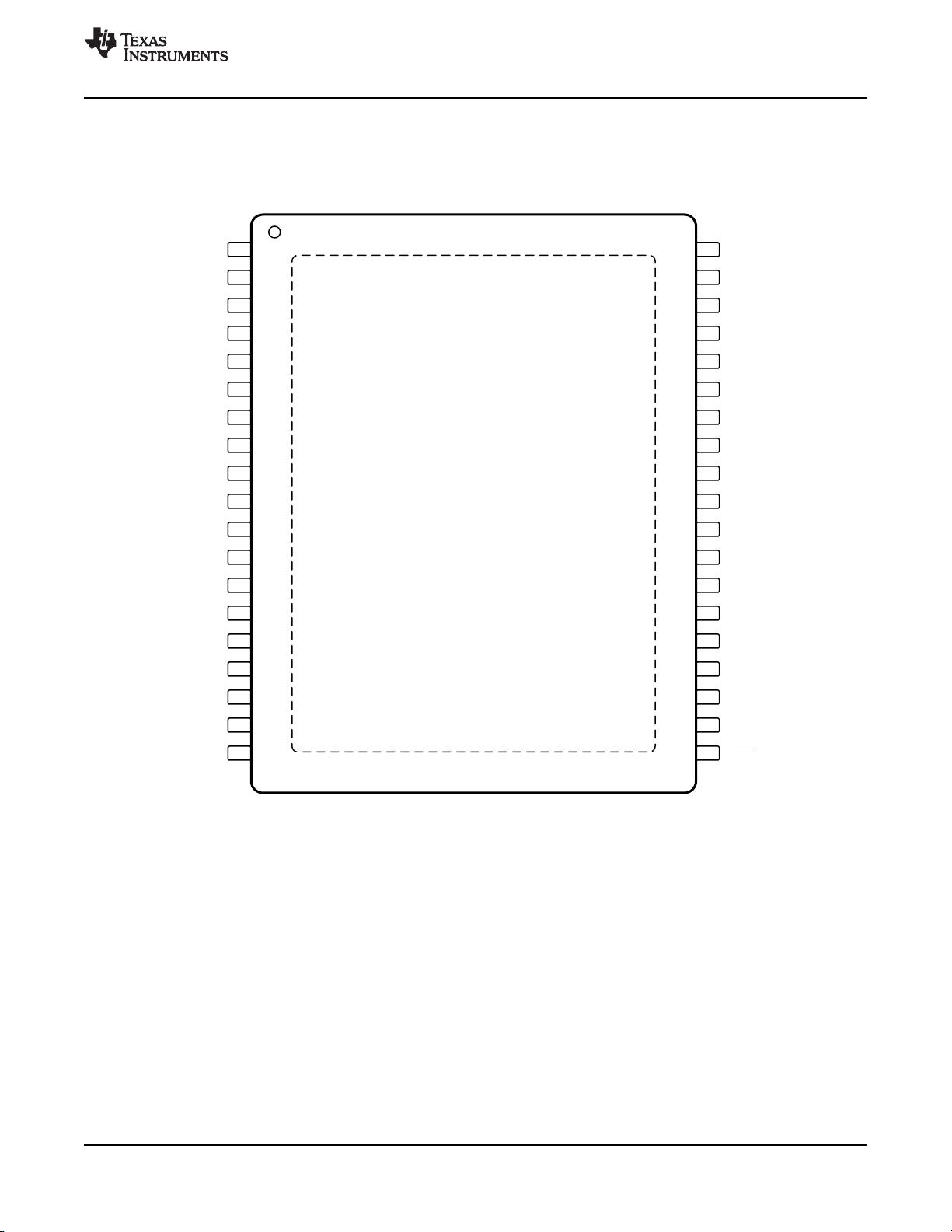
5 Pin Configuration and Functions......................... 3
6 Specifications......................................................... 4
6.1 Absolute Maximum Ratings ...................................... 4
6.2 ESD Ratings.............................................................. 4
6.3 Recommended Operating Conditions....................... 5
6.4 Thermal Information.................................................. 6
6.5 Electrical Characteristics........................................... 6
6.6 Timing Requirements................................................ 8
6.7 Switching Characteristics.......................................... 9
6.8 Typical Characteristics............................................ 20
7 Detailed Description............................................ 21
7.1 Overview ................................................................. 21
7.2 Functional Block Diagram ....................................... 21
7.3 Feature Description................................................. 22
7.4 Device Functional Modes........................................ 31
7.5 Programming .......................................................... 31
7.6 Register Maps......................................................... 37
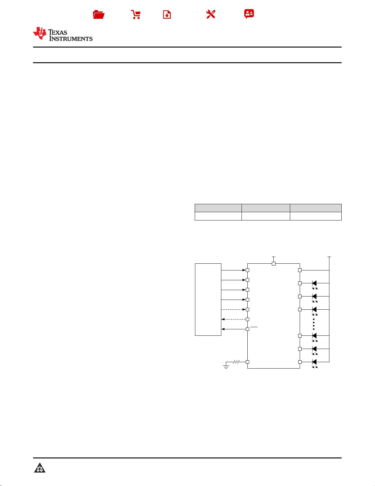
8 Application and Implementation ........................ 48
8.1 Application Information............................................ 48
8.2 Typical Application ................................................. 48
9 Power Supply Recommendations...................... 50
10 Layout................................................................... 50
10.1 Layout Guidelines ................................................. 50
10.2 Layout Example .................................................... 50
11 器器件件和和文文档档支支持持 ..................................................... 51
11.1 接收文档更新通知 ................................................. 51
11.2 社区资源................................................................ 51
11.3 商标 ....................................................................... 51
11.4 静电放电警告......................................................... 51
11.5 术语表 ................................................................... 51
12 机机械械、、封封装装和和可可订订购购信信息息....................................... 51
4 修修订订历历史史记记录录
Changes from Original (July 2018) to Revision A Page
• Changed the description for GCLK in .................................................................................................................................... 4
• Changed "indicates" to "initiates" in the Global Reset section ............................................................................................. 30
• Added "the SID" to the Fault Mode section to identify the register where the overtemperature fault is latched.................. 31
• Changed "APS time" to "APS detection time" for bit 199 in 表 12 ....................................................................................... 32
• Changed "24 zones" to "16 zones" and "six TLC6C5716-Q1 units" to "eight TLC6C5716-Q1 units" in the Detailed
Design Procedure section ................................................................................................................................................... 49
• Added a new sentence preceding 图 32 .............................................................................................................................. 49
• Added the Application Curves section.................................................................................................................................. 49
• Added two sentences to the Power Supply Recommendations section .............................................................................. 50
1SDI 38 SENSE
2SCK 37 NC
3LATCH 36 BLANK
4GCLK 35
V
CC
5GCLK 34 IREF
6GCLK 33 GND
7NU 32 NU
8OUTR0 31 OUTR7
9OUTB0 30 OUTB7
10NU 29 NU
11OUTR1 28 OUTR6
12OUTB1 27 OUTB6
13NU 26 NU
14OUTR2 25 OUTR5
15OUTB2 24 OUTB5
16NU 23 NU
17OUTR3 22 OUTR4
18OUTB3 21 OUTB4
19SDO 20 ERR
Not to scale
Thermal
Pad
3
TLC6C5716-Q1
www.ti.com.cn
ZHCSIG2A –JULY 2018–REVISED AUGUST 2018
Copyright © 2018, Texas Instruments Incorporated
5 Pin Configuration and Functions
DAP PowerPAD™ Package
38-Pin HTSSOP With Exposed Thermal Pad
Top View
NC – No internal connection
NU – Make no external connection
4
TLC6C5716-Q1
ZHCSIG2A –JULY 2018–REVISED AUGUST 2018
www.ti.com.cn
Copyright © 2018, Texas Instruments Incorporated
Pin Functions
PIN
I/O DESCRIPTION
NAME NO.
BLANK 36 I
Blank all outputs. BLANK low forces all channels off. The grayscale counter resets
and the grayscale PWM timing controller is initialized. BLANK high starts the
grayscale PWM timing controller. Channels are controlled by the PWM timing
controller.
ERR 20 O Open-drain error feedback
GCLK 4, 5, 6 I
Clock input for the grayscale PWM counter, three pins are internally connected
together
GND 33 — Power ground
IREF 34 I Reference-current pin for setting the full-scale output current
LATCH 3 I Latch-enable input pin
NC 37 — No internal connection
NU
7, 10, 13,16,
23, 26, 29, 32
— Not used, keep floating
OUTB0–OUTB7
9, 12, 15, 18,
21, 24, 27, 30
O Constant-current outputs for group B
OUTR0–OUTR7
8, 11, 14,17,
22, 25, 28, 31
O Constant-current outputs for group R
SCK 2 I Input pin for the data-shift clock
SDI 1 I Serial data-in pin
SDO 19 O Serial data-out pin
SENSE 38 I LED supply sensing pin
V
CC
35 I Power supply pin
Thermal pad — — Connect to ground to improve thermal performance
(1) Stresses beyond those listed under Absolute Maximum Ratings may cause permanent damage to the device. Theseare stress ratings
only, which do not imply functional operation of the device at these or anyother conditions beyond those indicated under Recommended
OperatingConditions. Exposure to absolute-maximum-rated conditions for extended periods mayaffect device reliability.
6 Specifications
6.1 Absolute Maximum Ratings
over operating junction temperature range (unless otherwise noted)
(1)
MIN MAX UNIT
Input voltage
V
CC
–0.3 6
VSENSE –0.3 8
BLANK, GCLK, LATCH, SCK, SDI –0.3 V
CC
+ 0.3
Output voltage
ERR, IREF, SDO –0.3 V
CC
+ 0.3
V
OUTR0–OUTR7, OUTB0–OUTB7 –0.3 8
Output current OUTR0–OUTR7, OUTB0–OUTB7 0 50 mA
Operating junction temperature, T
J
–40 150 °C
Storage temperature, T
stg
–55 150 °C
(1) AEC Q100-002 indicates that HBM stressing shall be in accordancewith the ANSI/ESDA/JEDEC JS-001 specification.
6.2 ESD Ratings
VALUE UNIT
V
(ESD)
Electrostatic discharge
Human-body model (HBM), per AEC Q100-002,
(1)
HBM ESD classification level H2
±2000
V
Charged-device model (CDM), AEC Q100
classification C4B, per AEC Q100-011
All pins ±500
Corner pins ±750
5
TLC6C5716-Q1
www.ti.com.cn
ZHCSIG2A –JULY 2018–REVISED AUGUST 2018
Copyright © 2018, Texas Instruments Incorporated
6.3 Recommended Operating Conditions
over operating junction temperature range (unless otherwise noted)
MIN NOM MAX UNIT
V
CC
Device supply voltage 3 5.5 V
V
SENSE
LED supply voltage 8 V
V
O
Output voltage 8 V
V
IL
Input logic-low voltage BLANK, GCLK, LATCH, SCK, SDI 0 0.3 V
CC
V
V
IH
Input logic-high voltage BLANK, GCLK, LATCH, SCK, SDI 0.7 V
CC
V
CC
V
I
OH
High-level output current SDO 1 mA
I
OL
Low-level input current
SDO 1 mA
ERR 5 mA
I
O
Constant output sink current OUTR0–OUTR7, OUTB0–OUTB7 2 50 mA
T
A
Operating ambient temperature –40 125 °C
T
J
Operating junction temperature –40 150 °C
剩余54页未读,继续阅读
安全验证
文档复制为VIP权益,开通VIP直接复制
信息提交成功
评论0
最新资源