TI-TLC6C5712-Q1.pdf
需积分: 9 130 浏览量
2022-11-16
23:51:17
上传
评论 5
收藏 2.12MB PDF 举报


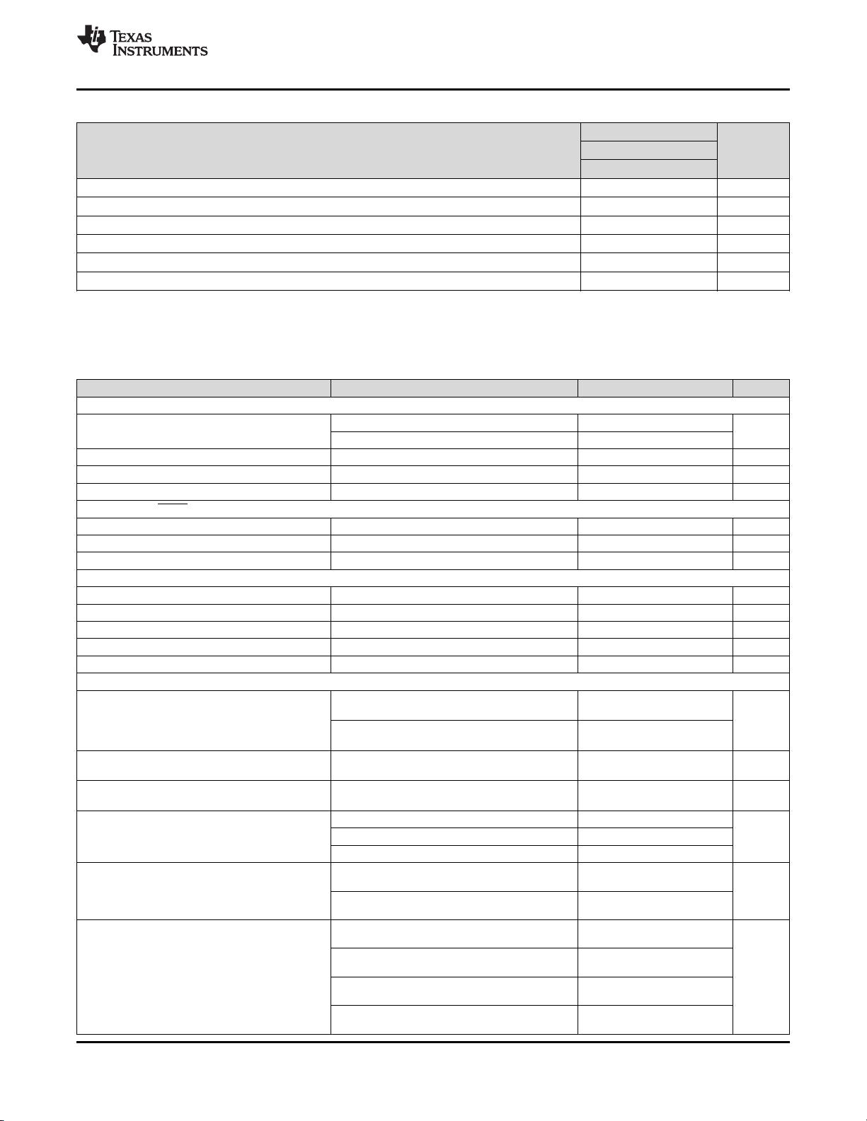
3-V to 5.5-V
Supply Voltage
GND
OUT0
TLC6C5712-Q1
IREF
SDI
SCK
V
(SUPPLY)
V
CC
V
F
OUT11
SENSE
LATCH
OUT1
SDO
R
(IREF)
ERR
PWM5
PWM0
OUT10
OUT9
Product
Folder
Sample &
Buy
Technical
Documents
Tools &
Software
Support &
Community
An IMPORTANT NOTICE at the end of this data sheet addresses availability, warranty, changes, use in safety-critical applications,
intellectual property matters and other important disclaimers. PRODUCTION DATA.
English Data Sheet: SLVSCO9
TLC6C5712-Q1
ZHCSEM2A –AUGUST 2015–REVISED AUGUST 2015
TLC6C5712-Q1 具具有有 8 位位点点校校正正功功能能的的 12 通通道道全全套套诊诊断断、、恒恒定定灌灌电电流流
LED 驱驱动动器器
1
1 特特性性
1
• 适用于汽车电子 应用
• 符合 AEC-Q100 标准
– 器件温度等级 1:环境运行温度范围为 -40°C
至 125°C
– 器件人体放电模式 (HBM) 静电放电 (ESD) 分类
等级 H3A
– 器件组件充电模式 (CDM) ESD 分类等级 C4B
• 12 条功率双扩散金属氧化物半导体 (DMOS) 晶体
管输出通道
– 最大恒定电流高达 75mA,可通过外部电阻进行
编程
– 最高输出电压高达 7V
– 最高压降电压:
– 50mA 时为 0.75V/通道
– 75mA 时为 1.2V/通道
• 出色的输出恒流精度:
– 通道间的差异:< ±3%(最大值)
– 器件间的差异:< ±3%(最大值)
– 每通道 8 位、256 步长线性点校正
• 支持灵活的外部脉宽调制 (PWM) 调光
– 6 个具有频率监控功能的 PWM 输入
– 通过串行外设接口 (SPI) 实现可编程通道映射
• 保护和诊断
– 相邻引脚短路检测
– 在激活和禁用状态下可检测开路负载、短接至地
以及发光二极管 (LED) 短路
– 热预警与热关断
– 开漏错误报告
– LED 弱电源诊断
– 参考电阻开路或短路检测与保护
– 通过 SPI 寄存器锁定实现内容保护
– SPI 完整性诊断的强制错误
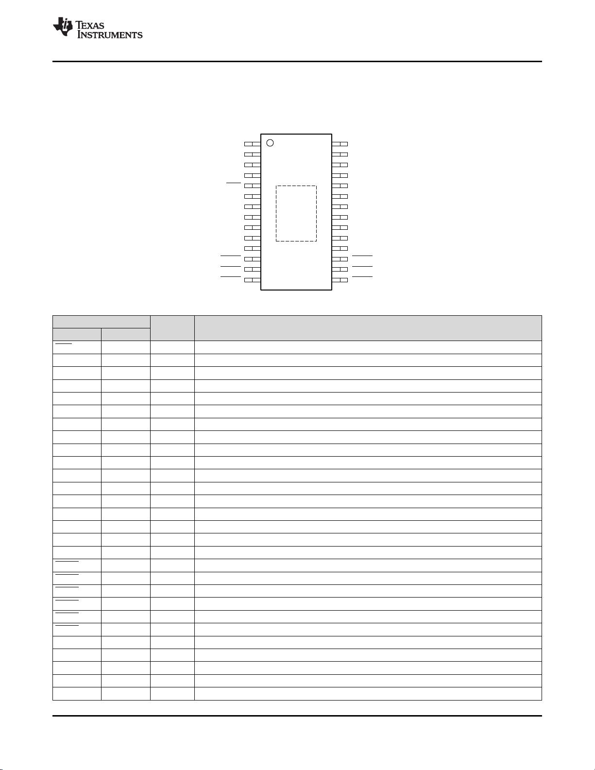
• 小型热有效的 28 引脚散热薄型小外形尺寸
(HTSSOP) 封装 PowerPAD™封装
2 应应用用范范围围
• 仪表板信号装置指示灯
• 面板及按钮背光照明
• 条形图 LED
• 变速器 PRNDL 档位指示灯
• 连续转向指示灯
3 说说明明
在汽车仪表板及其他安全性能至关重要的 LED 驱动器
应用中,为了确保 LED 亮度与色温的一致性,针对多
通道 LED 的性能需求日益提升。系统级安全考量因素
要求检测各种故障情况,因此会加深系统的复杂程度。
TLC6C5712-Q1 器件是一款 12 通道恒定灌电流 LED
驱动器。凭借 8 位点校正功能和高精度输出电
流,TLC6C5712-Q1 器件成为校正 LED 亮度和色温变
化的理想解决方案。该器件针对每个组件提供高级保护
和诊断功能,可提升系统级稳定性并简化面向安全的设
计。六个具有可编程映射功能的 PWM 输入支持多种
LED 颜色调光配置并提供高调光比率。具有诊断功能
的 16 位串行外设接口 (SPI) 支持以菊花链方式连接多
个器件并简化系统级设计。
器器件件信信息息
(1)
器器件件型型号号 封封装装 封封装装尺尺寸寸((标标称称值值))
TLC6C5712-Q1 HTSSOP (28) 4.40mm x 9.70mm
(1) 要了解所有可用封装,请见数据表末尾的可订购产品附录。
典典型型应应用用电电路路原原理理图图

剩余68页未读,继续阅读
资源评论


