TI-TLC6C5912-Q1.pdf
需积分: 9 136 浏览量
2022-11-16
23:50:14
上传
评论 5
收藏 1.53MB PDF 举报

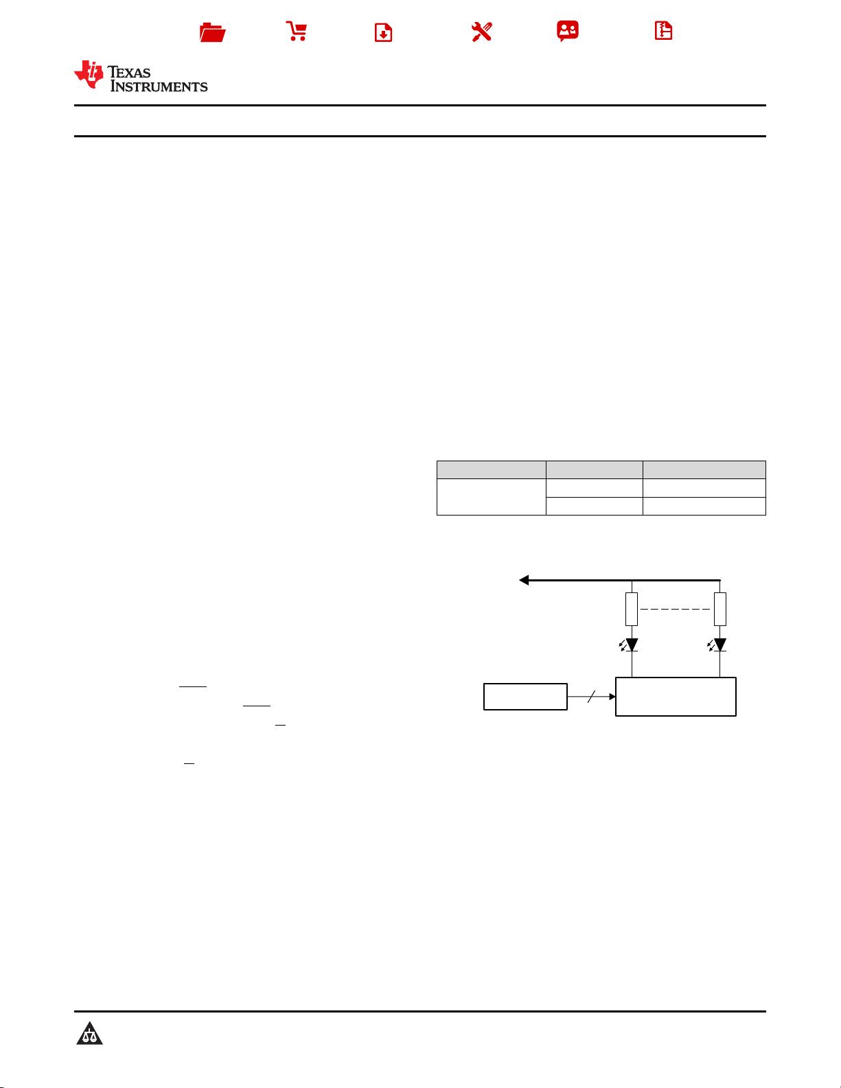
30 mA30 mA
4/3
12-Bit Shift Register
LED Driver
MCU Serial I/F
Battery 9 V–40 V
Product
Folder
Sample &
Buy
Technical
Documents
Tools &
Software
Support &
Community
Reference
Design
An IMPORTANT NOTICE at the end of this data sheet addresses availability, warranty, changes, use in safety-critical applications,
intellectual property matters and other important disclaimers. PRODUCTION DATA.
English Data Sheet: SLIS141
TLC6C5912-Q1
ZHCS301C –DECEMBER 2012–REVISED JULY 2016
TLC6C5912-Q1 电电源源逻逻辑辑 12 通通道道移移位位寄寄存存器器 LED 驱驱动动器器
1
1 特特性性
1
• 适用于汽车电子 应用
• 宽 V
CC
电压范围:3.5V 至 5.5V
• 40V 的最大输出额定值
• 12 个功率 DMOS 晶体管输出,
V
CC
= 5V 时的连续电流输出达 50mA
• 热关断保护
• 针对多级的增强型级联
• 所有寄存器由单一输入清零
• 低功耗
• 缓开关时间(t
r
和 t
f
),这十分有助于减少电磁干扰
(EMI)
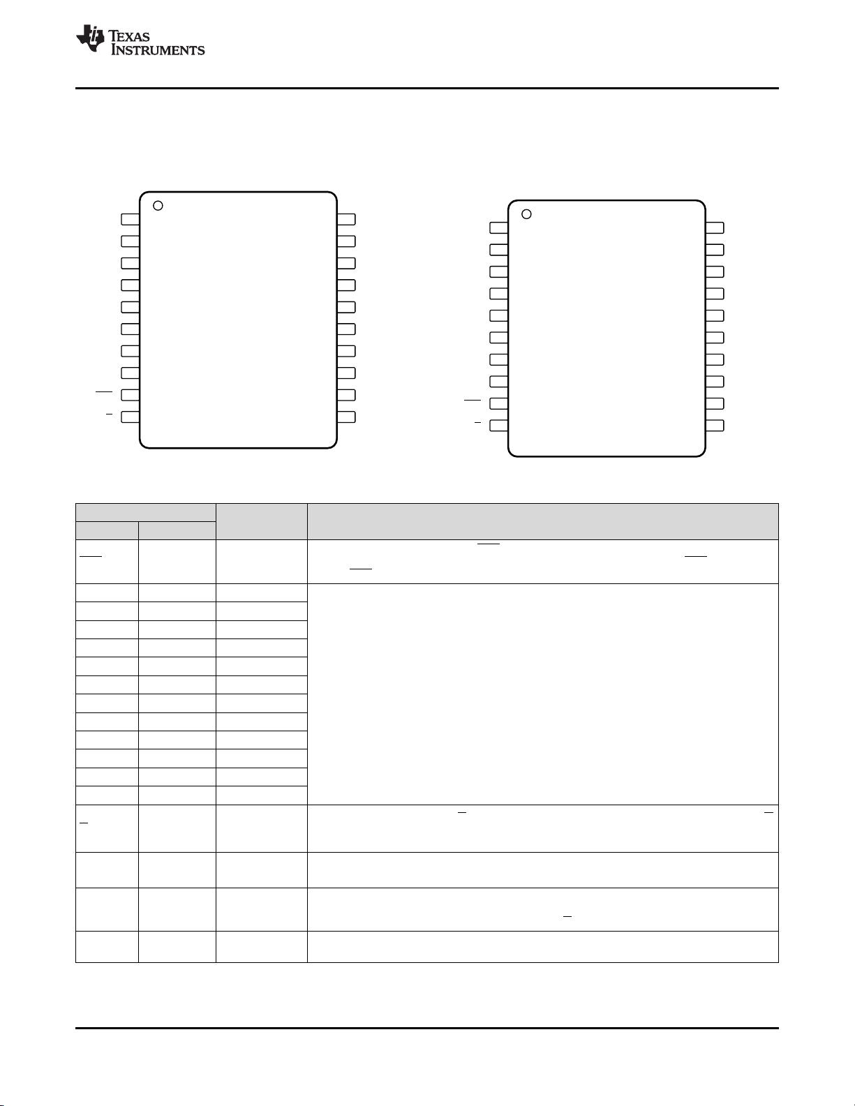
• 20 引脚薄型小外形尺寸 (TSSOP)-PW 封装
• 20 引脚 DW 封装
2 应应用用
• 仪表板
• 信号灯
• LED 照明和控制
3 说说明明
TLC6C5912-Q1 是一款单片、中等电压、低电流电源
12 位移位寄存器,设计用于需要相对适量负载功率的
系统(如 LED)中。
此器件包含一个 12 位串入、并出移位寄存器,此寄存
器为一个 12 位 D 类存储寄存器提供数据。移位和存
储寄存器之间的数据传输分别在移位寄存器时钟
(SRCK) 和寄存器时钟 (RCK) 的上升边沿上发生。当
移位寄存器清零 (CLR) 为高电平时,存储寄存器将数
据传输到输出缓冲器 。一个CLR上的低电平将器件中
的所有寄存器清零。将输出使能 (G) 保持为高电平将
把输出缓冲器中的所有数据保存为低电平,并且所有漏
极输出关闭。保持G为低电平将使得来自存储寄存器中
的数据对于输出缓冲器不可见。
当输出缓冲器中的数据为低电平时,DMOS 晶体管的
输出被关闭。当数据为高电平时,DMOS 晶体管输出
具有电流吸收功能。串行输出 (SER OUT) 在 SRCK
的下降沿随时钟移出器件,为级联应用提供更多保持
时间。这对于时钟信号可能出现偏移的应用、 放置位
置相互不靠近的器件、 或者电磁干扰较大的系统而言
可以提升性能。此器件内置有热关断保护。
输出端为低侧开漏 DMOS 晶体管,输出额定电压为
40V,V
CC
= 5V 时拥有 50mA 的连续灌电流能力。电
流限值随着结温上升而降低,从而提供额外的器件保
护。该器件还提供高达 2000V 的 ESD 人体模型保护
和 200V 的 ESD 机器模型保护。
TLC6C5912-Q1 的额定运行环境温度范围为 -40°C 至
125°C。
器器件件信信息息
(1)
器器件件型型号号 封封装装 封封装装尺尺寸寸((标标称称值值))
TLC6C5912-Q1
SOIC (20) 12.80mm x 7.50mm
TSSOP (20) 6.50mm × 4.40mm
(1) 要了解所有可用封装,请参见数据表末尾的可订购产品附录。
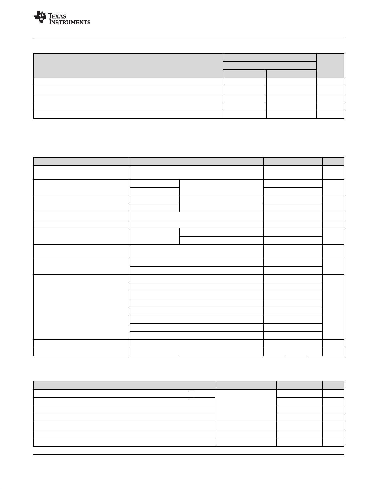
典典型型应应用用电电路路原原理理图图
剩余26页未读,继续阅读


评论0
最新资源