
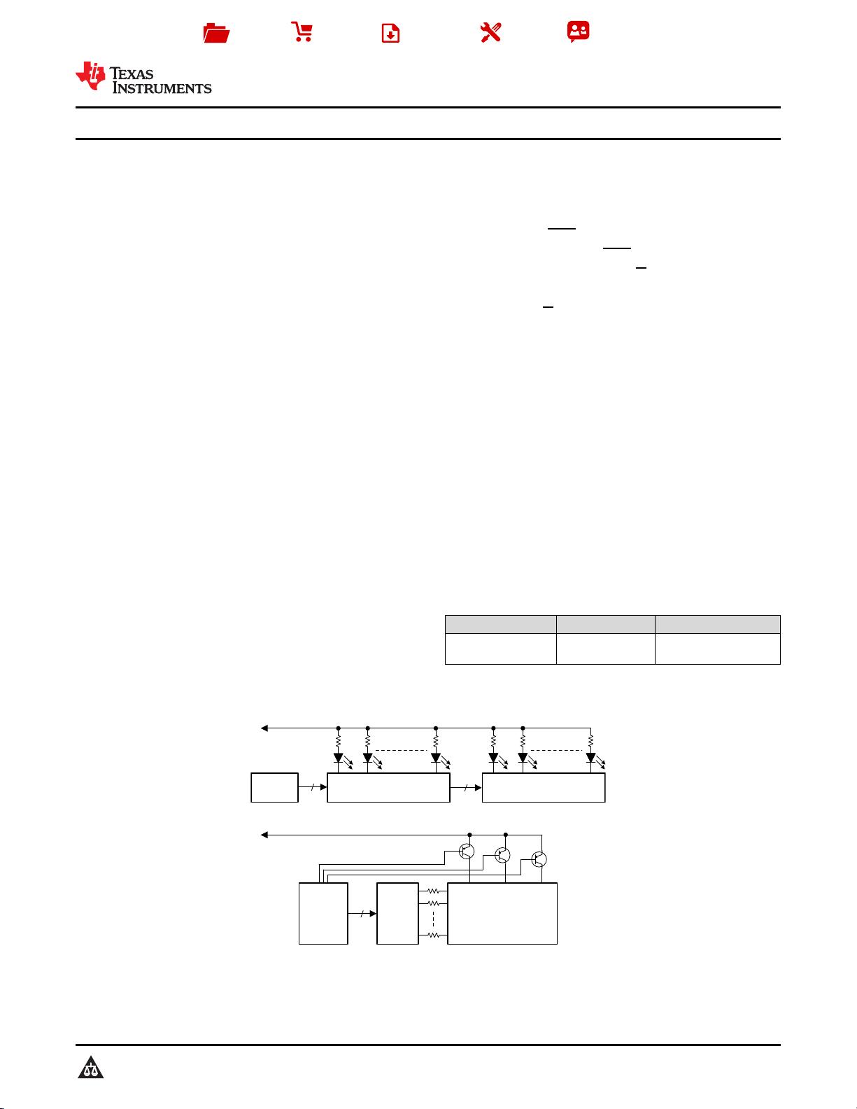
12-Bit Shift Register
LED Driver
Power Supply
4/3
4/3
Typical Cascade Topology
12-Bit Shift Register
LED Driver
MCU Serial
Interface
12-Bit Shift-
Register
LED Driver
3 12 LED Matrix´
4/3
I/Os
Power Supply
Typical Scan Topology
MCU Serial
Interface
Copyright © 2016, Texas Instruments Incorporated
Product
Folder
Sample &
Buy
Technical
Documents
Tools &
Software
Support &
Community
An IMPORTANT NOTICE at the end of this data sheet addresses availability, warranty, changes, use in safety-critical applications,
intellectual property matters and other important disclaimers. PRODUCTION DATA.
English Data Sheet: SLIS180
TLC6C5912
ZHCSF22 –MAY 2016
TLC6C5912 12 通通道道移移位位寄寄存存器器 LED 驱驱动动器器
1
1 特特性性
1
• 3V 至 5.5V 宽 V
CC
范围
• 40V 最大额定输出
• 12 路功率双扩散金属氧化物半导体 (DMOS) 晶体
管输出:
50mA 持续电流 (V
CC
= 5V) 或者
200mA 脉宽调制 (PWM) 电流(单脉冲持续时间短
于 1ms 且平均电流低于 50mA
r
)
• 热关断保护
• 针对多级的增强型级联
• 所有寄存器由单一输入清零
• 低功耗
• 缓慢开关时间(t 和 t
f
),非常有助于减少电磁干扰
(EMI)
• 20 引脚薄型小外形尺寸 (TSSOP)-PW 封装
2 应应用用
• 电器显示面板
• 电梯显示面板
• PLC 功能指示器
• 七段显示器
3 说说明明
TLC6C5912 是一款单片、中等电压、低电流功率 12
位移位寄存器,专为负载功率要求相对适中的系统(例
如 LED)而设计。
此器件包含一个 12 位串入、并出移位寄存器,此寄存
器为一个 12 位 D 类存储寄存器提供数据。移位和存
储寄存器之间的数据传输分别在移位寄存器时钟
(SRCK) 和寄存器时钟 (RCK) 的上升边沿上发生。当
移位寄存器清零(CLR) 为高电平时,存储寄存器将数据
传输到输出缓冲器 。一个CLR上的低电平将器件中的
所有寄存器清零。将输出使能 (G) 保持为高电平将把
输出缓冲器中的所有数据保存为低电平,并且所有漏极
输出关闭。保持G为低电平将使得来自存储寄存器中的
数据对于输出缓冲器不可见。
该器件包含一个 12 位串入并出移位寄存器。该寄存器
为一个 12 位 D 类存储寄存器提供数据。移位寄存器
和存储寄存器各自具备独立时钟。
输出为低侧、漏极开路 DMOS 晶体管输出:额定输出
为 40V 及 50mA 持续灌电流或者 200mA PWM 电流
(V
CC
= 5V 时,单脉冲持续时间短于 1ms 且平均电流
低于 50mA)。该器件内置热关断保护,在人体模型和
200V 机器模型测试中可提供高达 2000V 的静电放电
(ESD) 保护。
TLC6C5912 的额定工作环境温度范围为 -40°C 至
105°C。
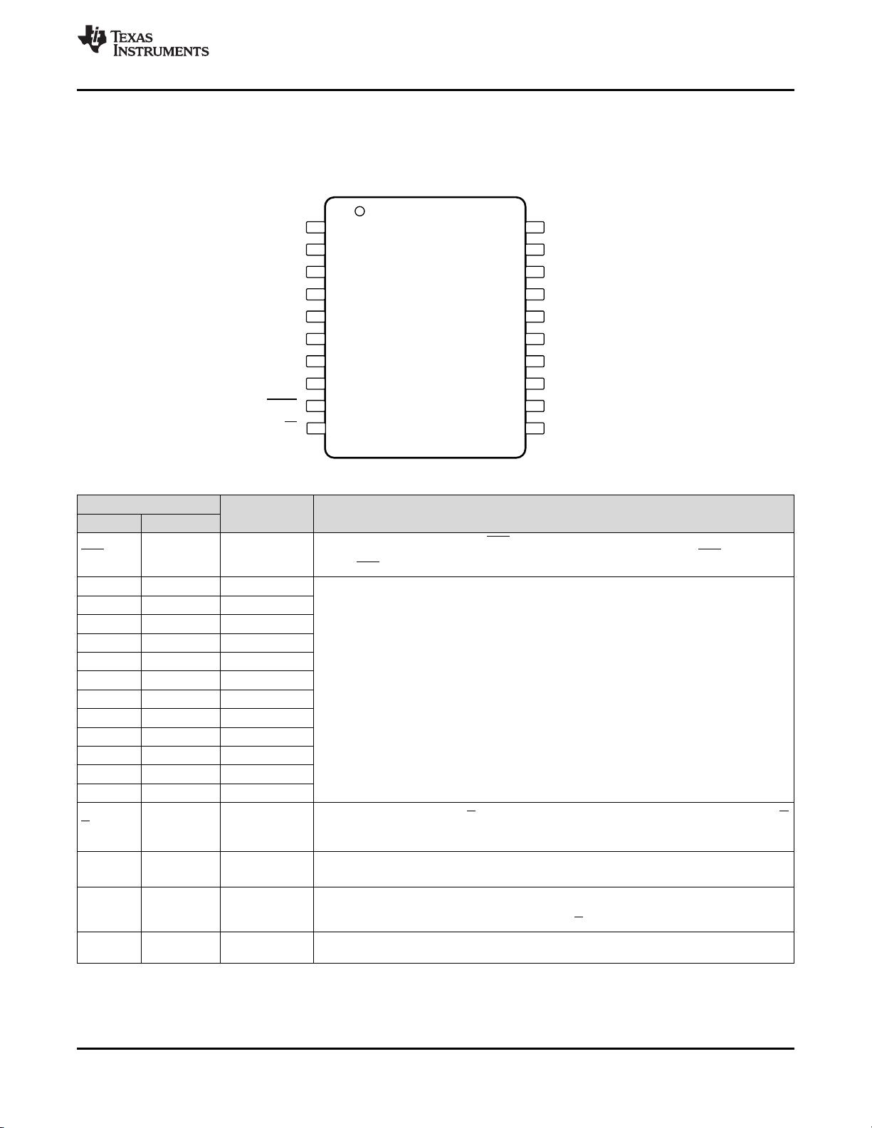
器器件件信信息息
(1)
器器件件型型号号 封封装装 封封装装尺尺寸寸((标标称称值值))
TLC6C5912
薄型小外形尺寸封
装 (TSSOP) (20)
6.50mm x 4.40mm
(1) 要了解所有可用封装,请见数据表末尾的可订购产品附录。
典典型型应应用用电电路路原原理理图图
剩余20页未读,继续阅读
资源评论


不觉明了
- 粉丝: 6292
- 资源: 5764


最新资源
- 【多智能体控制】基于matlab自适应领导者与追随者动态规划仿真【含Matlab源码 8003期】.mp4
- 压合半自动组装线体工程图机械结构设计图纸和其它技术资料和技术方案非常好100%好用.zip
- 移动式液压伸缩提升机工程图机械结构设计图纸和其它技术资料和技术方案非常好100%好用.zip
- sgg慕尚花坊项目代码
- 折弯激光焊接设备工程图机械结构设计图纸和其它技术资料和技术方案非常好100%好用.zip
- 已生产的插针机工程图机械结构设计图纸和其它技术资料和技术方案非常好100%好用.zip
- 纸盒成型机工程图机械结构设计图纸和其它技术资料和技术方案非常好100%好用.zip
- 智能仓库穿梭车工程图机械结构设计图纸和其它技术资料和技术方案非常好100%好用.zip
- 纸盒六面包膜机覆膜机工程图机械结构设计图纸和其它技术资料和技术方案非常好100%好用.zip
- 自动Mylar贴合机工程图机械结构设计图纸和其它技术资料和技术方案非常好100%好用.zip
- 自动裁切机工程图机械结构设计图纸和其它技术资料和技术方案非常好100%好用.zip
- 自动调节双轴变位机单边基座工程图机械结构设计图纸和其它技术资料和技术方案非常好100%好用.zip
- 自动裁布机工程图机械结构设计图纸和其它技术资料和技术方案非常好100%好用.zip
- 自动焊管机工程图机械结构设计图纸和其它技术资料和技术方案非常好100%好用.zip
- 自制点胶系统工程图机械结构设计图纸和其它技术资料和技术方案非常好100%好用.zip
- 自动覆膜设备工程图机械结构设计图纸和其它技术资料和技术方案非常好100%好用.zip
资源上传下载、课程学习等过程中有任何疑问或建议,欢迎提出宝贵意见哦~我们会及时处理!
点击此处反馈


