
TLC5510, TLC5510A
8-BIT HIGH-SPEED ANALOG-TO-DIGITAL CONVERTERS
SLAS095L – SEPTEMBER 1994 – REVISED JUNE 2003
1
POST OFFICE BOX 655303 • DALLAS, TEXAS 75265
features
D
Analog Input Range
– TLC5510 ...2 V Full Scale
– TLC5510A ...4 V Full Scale
D
8-Bit Resolution
D
Integral Linearity Error
±0.75 LSB Max (25°C)
±1 LSB Max (–20°C to 75°C)
D
Differential Linearity Error
±0.5 LSB Max (25°C)
±0.75 LSB Max (–20°C to 75°C)
D
Maximum Conversion Rate
20 Mega-Samples per Second
(MSPS) Max
D
5-V Single-Supply Operation
D
Low Power Consumption
TLC5510 . . . 127.5 mW Typ
TLC5510A . . . 150 mW Typ
(includes reference resistor dissipation)
D
TLC5510 is Interchangeable With Sony
CXD1175
applications
D
Digital TV
D
Medical Imaging
D
Video Conferencing
D
High-Speed Data Conversion
D
QAM Demodulators
description
The TLC5510 and TLC5510A are CMOS, 8-bit, 20
MSPS analog-to-digital converters (ADCs) that
utilize a semiflash architecture. The TLC5510 and
TLC5510A operate with a single 5-V supply and
typically consume only 130 mW of power.
Included is an internal sample-and-hold circuit,
parallel outputs with high-impedance mode, and
internal reference resistors.
The semiflash architecture reduces power
consumption and die size compared to flash
converters. By implementing the conversion in a
2-step process, the number of comparators is
significantly reduced. The latency of the data
output valid is 2.5 clocks.
The TLC5510 uses the three internal reference
resistors to create a standard, 2-V, full-scale
conversion range using V
DDA
. Only external jumpers are required to implement this option and eliminates the
need for external reference resistors. The TLC5510A uses only the center internal resistor section with an
externally applied 4-V reference such that a 4-V input signal can be used. Differential linearity is 0.5 LSB at 25°C
and a maximum of 0.75 LSB over the full operating temperature range. Typical dynamic specifications include
a differential gain of 1% and differential phase of 0.7 degrees.
The TLC5510 and TLC5510A are characterized for operation from –20°C to 75°C.
AVAILABLE OPTIONS
PACKAGE
MAXIMUM FULL SCALE
T
A
TSSOP (PW)
SOP (NS)
(TAPE AND REEL ONLY)
MAXIMUM
FULL
-
SCALE
INPUT VOLTAGE
20°Cto75°C
TLC5510IPW TLC5510INSLE 2 V
–
20°C
to
75°C
– TLC5510AINSLE 4 V
Please be aware that an important notice concerning availability, standard warranty, and use in critical applications of
Texas Instruments semiconductor products and disclaimers thereto appears at the end of this data sheet.
Copyright 1994 – 2003, Texas Instruments Incorporated
PRODUCTION DATA information is current as of publication date.
Products conform to specifications per the terms of Texas Instruments
standard warranty. Production processing does not necessarily include
testing of all parameters.
1
2
3
4
5
6
7
8
9
10
11
12
24
23
22
21
20
19
18
17
16
15
14
13
OE
DGND
D1(LSB)
D2
D3
D4
D5
D6
D7
D8(MSB)
V
DDD
CLK
DGND
REFB
REFBS
AGND
AGND
ANALOG IN
V
DDA
REFT
REFTS
V
DDA
V
DDA
V
DDD
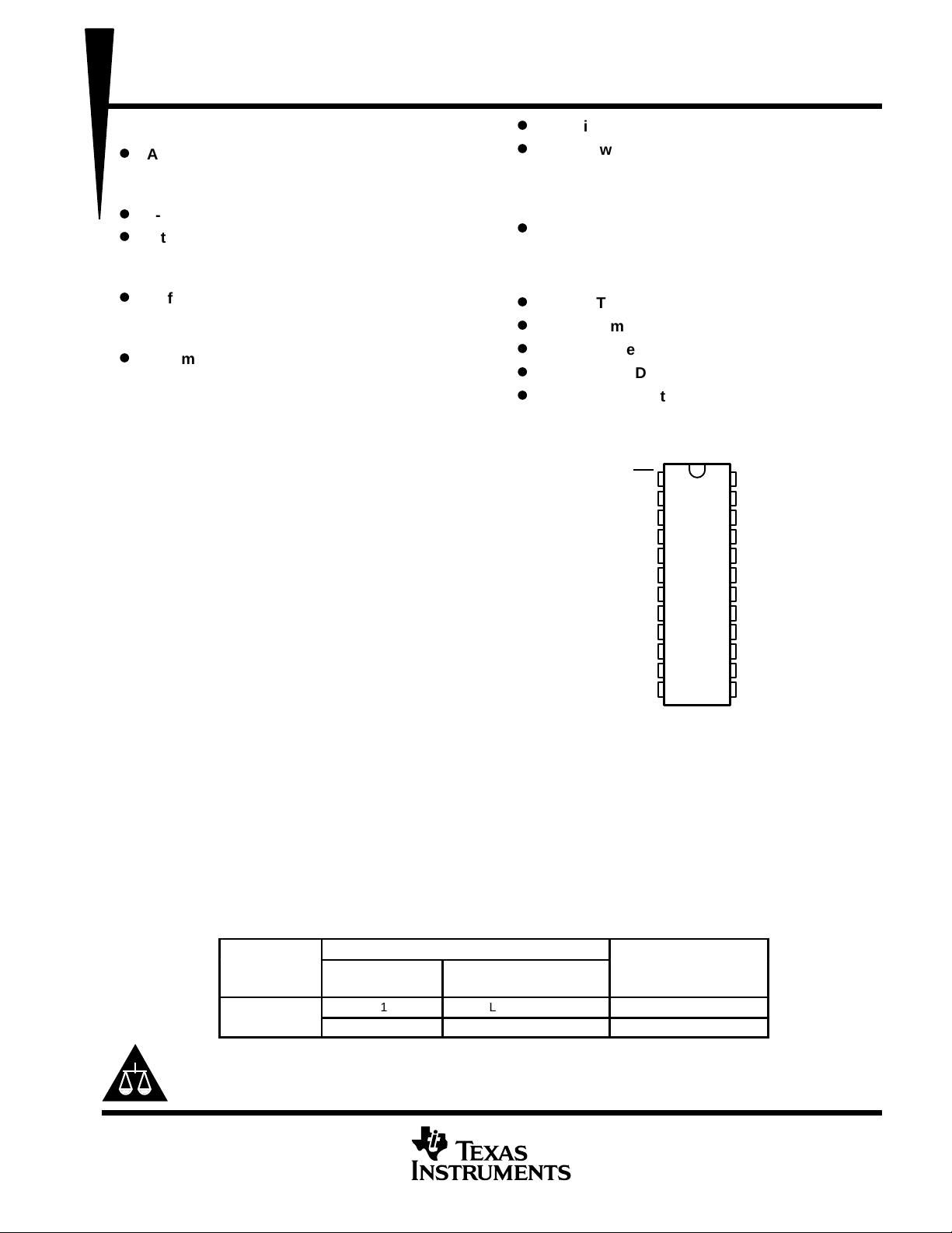
PW OR NS PACKAGE
†
(TOP VIEW)
†
Available in tape and reel only and ordered
as the shown in the Available Options table
below.

剩余20页未读,继续阅读


评论0
最新资源