TI-DS92LV2421.pdf
需积分: 11 156 浏览量
2023-02-08
23:01:32
上传
评论 4
收藏 1.77MB PDF 举报

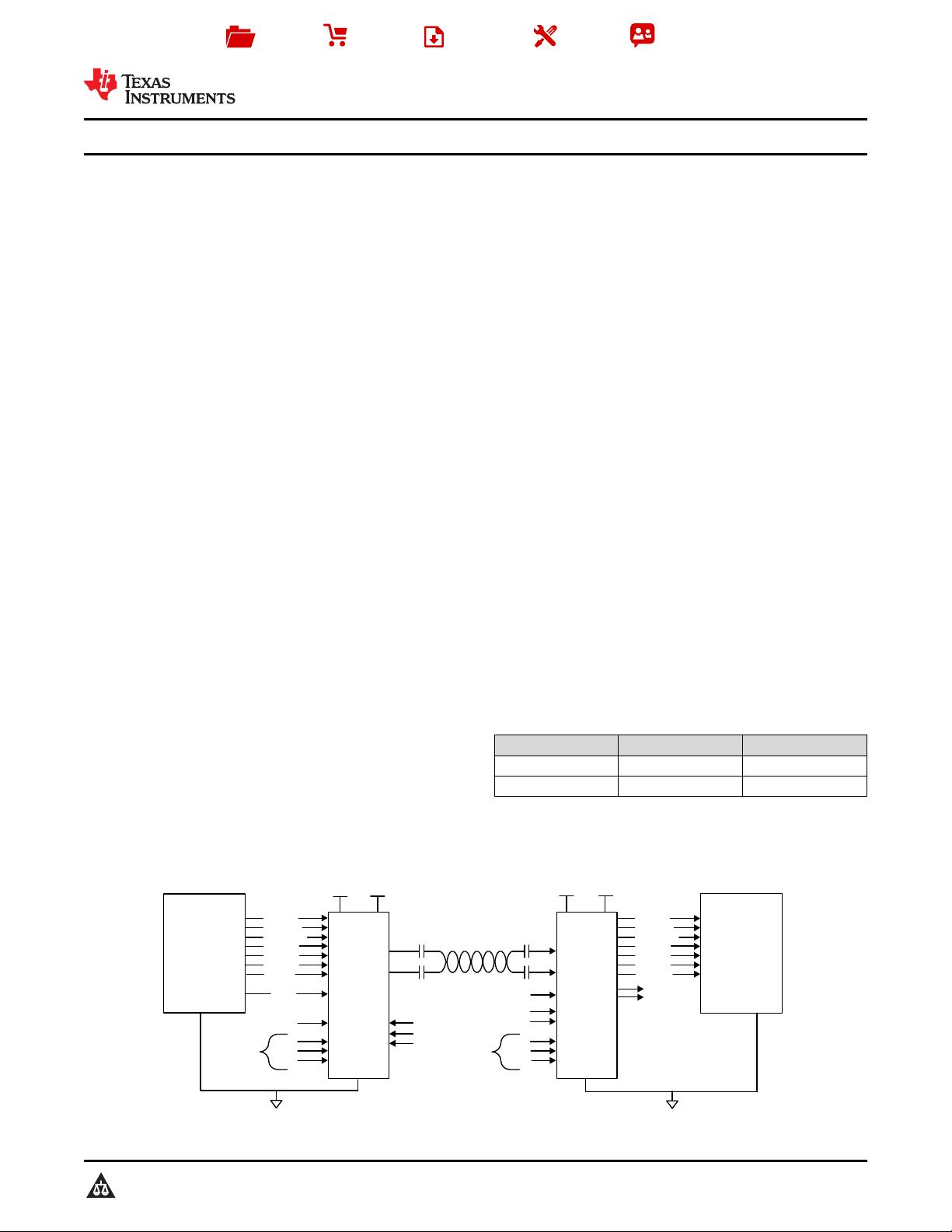
DI[7:0]
CI2
CI3
CLKIN
PDB
Serializer Deserializer
CI1
Graphic
Processor
Channel Link II
1 Pair / AC Coupled
DS92LV2421 DS92LV2422
100 ohm STP Cable
PASS
V
DDIO
PDB
SCL
SDA
RFB
VODSEL
DeEmph
BISTEN
BISTEN
LOCK
ID[x]
DAP DAP
CMF
100 nF 100 nF
SCL
SDA
ID[x]
STRAP pins
not shown
RIN+
RIN-
DOUT+
DOUT-
Optional Optional
(1.8V or 3.3V)(1.8V or 3.3V)
1.8V
1.8V
V
DDIO
V
DDn
V
DDn
ASIC/FPGA
OR
24-bit RGB
Display
ASIC/FPGA
OR
DI[15:8]
DI[23:16]
DO[7:0]
CO2
CO3
CLKOUT
CO1
DO[15:8]
DO[23:16]
Video
Imager
OR
Copyright © 2016, Texas Instruments Incorporated
Product
Folder
Sample &
Buy
Technical
Documents
Tools &
Software
Support &
Community
An IMPORTANT NOTICE at the end of this data sheet addresses availability, warranty, changes, use in safety-critical applications,
intellectual property matters and other important disclaimers. PRODUCTION DATA.
DS92LV2421
,
DS92LV2422
SNLS321C –MAY 2010–REVISED MAY 2016
DS92LV242x 10-MHz to 75-MHz, 24-Bit Channel Link II Serializer And Deserializer
1
1 Features
1
• 24-Bit Data, 3-Bit Control, 10- to 75-MHz Clock
• AC-Coupled STP Interconnect Cable up to 10 m
• Integrated Terminations on Serializer and
Deserializer
• At-Speed Link BIST Mode and Reporting Pin
• Optional I
2
C-Compatible Serial Control Bus
• Power-Down Mode Minimizes Power Dissipation
• 1.8-V or 3.3-V Compatible LVCMOS I/O Interface
• –40° to 85°C Temperature Range
• >8-kV HBM
• Serializer (DS92LV2421)
– Data Scrambler for Reduced EMI
– DC-Balance Encoder for AC Coupling
– Selectable Output VOD and Adjustable
De-emphasis
• Deserializer (DS92LV2422)
– Fast Random Data Lock; No Reference Clock
Required
– Adjustable Input Receiver Equalization
– LOCK (Real-Time Link Status) Reporting Pin
– EMI Minimization on Output Parallel Bus
(SSCG)
– Output Slew Control (OS)
2 Applications
• Embedded Videos and Displays
• Medical Imaging and Factory Automation
• Office Automation (Printers and Scanners)
• Security and Video Surveillance
• General-Purpose Data Communication
3 Description
The DS92LV242x chipset translates a parallel 24–bit
LVCMOS data interface into a single high-speed CML
serial interface with embedded clock information. This
single serial stream eliminates skew issues between
clock and data, reduces connector size, and reduces
interconnect cost for transferring a 24-bit or less bus
over FR-4 printed-circuit board backplanes and
balanced cables. In addition, the DS92LV242x
chipset also features a 3-bit control bus for slow
speed signals. This allows for video and display
applications with up to 24 bits per pixel (RGB).
Programmable transmit de-emphasis, receive
equalization, on-chip scrambling, and DC balancing
enables longer distance transmission over lossy
cables and backplanes. The DS92LV2422
automatically locks to incoming data without an
external reference clock or special sync patterns,
providing easy plug-and-go operation. EMI is
minimized by the use of low voltage differential
signaling, receiver drive strength control, and spread
spectrum clocking capability.
The DS92LV242x chipset is programmable though an
I
2
C interface as well as through pins. A built-in, at-
speed BIST feature validates link integrity and may
be used for system diagnostics. The DS92LV2421 is
offered in a 48-pin WQFN, and the DS92LV2422 is
offered in a 60-pin WQFN package. Both devices
operate over the full industrial temperature range of
–40°C to 85°C.
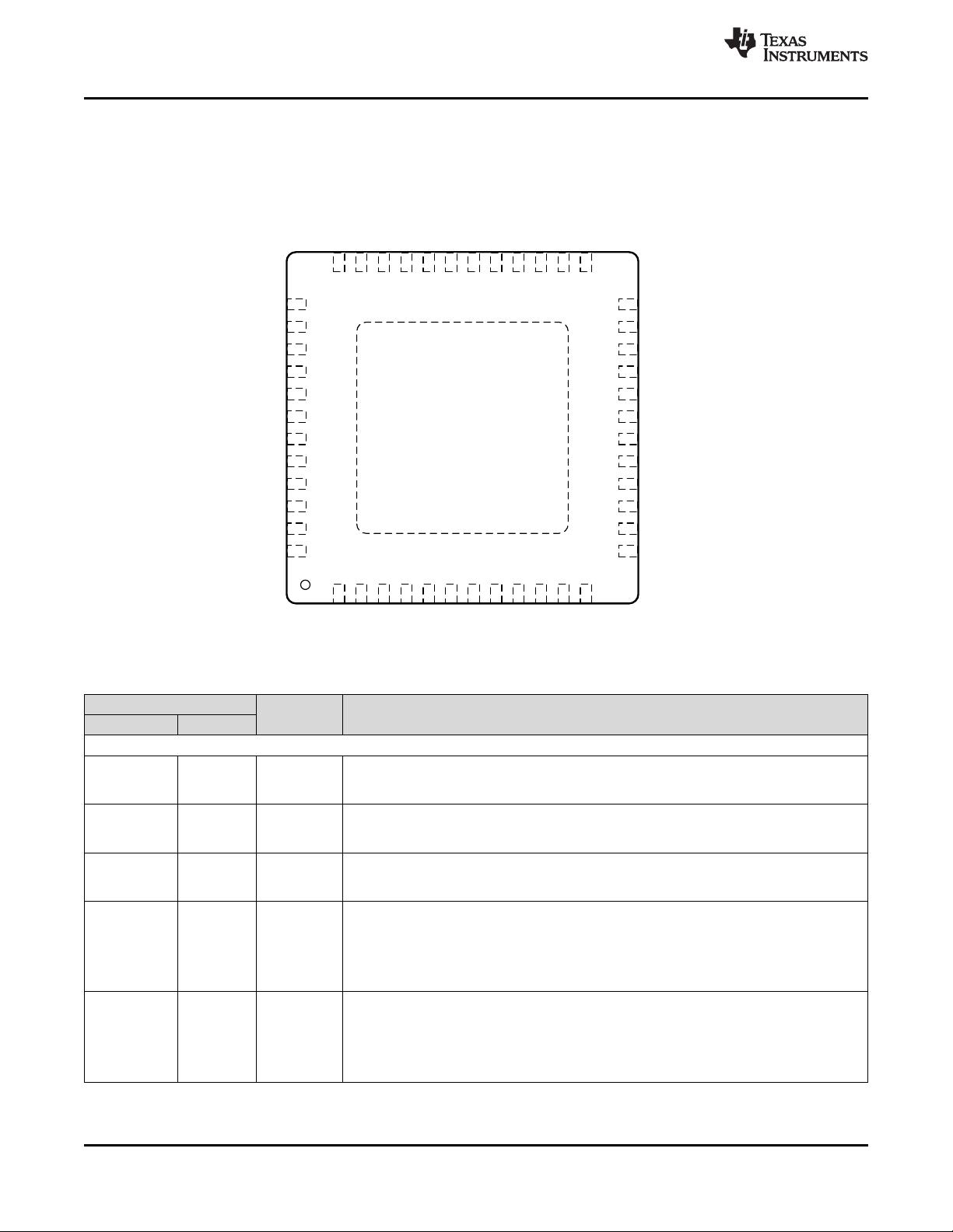
Device Information
(1)
PART NUMBER PACKAGE BODY SIZE (NOM)
DS92LV2421 WQFN (48) 7.00 mm × 7.00 mm
DS92LV2422 WQFN (60) 9.00 mm × 9.00 mm
(1) For all available packages, see the orderable addendum at
the end of the data sheet.
Typical Application Block Diagram

剩余62页未读,继续阅读
资源评论


