没有合适的资源?快使用搜索试试~ 我知道了~
TI-DS92LV8028.pdf
需积分: 8 0 下载量 196 浏览量
2023-02-08
23:00:34
上传
评论 4
收藏 724KB PDF 举报
温馨提示
试读
22页
LVDS串行器
资源推荐
资源详情
资源评论
DS92LV8028
www.ti.com
SNLS152I –NOVEMBER 2001–REVISED APRIL 2013
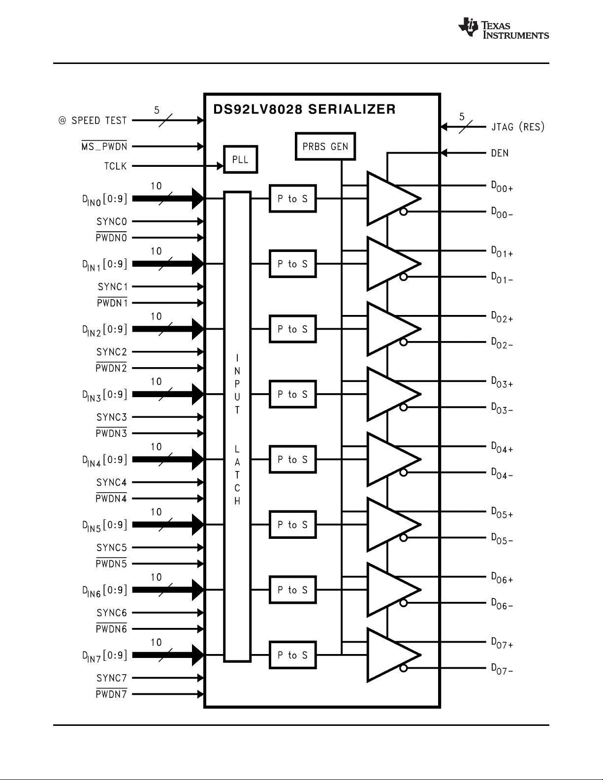
DS92LV8028 8 Channel 10:1 Serializer
Check for Samples: DS92LV8028
1
FEATURES
DESCRIPTION
The DS92LV8028 integrates eight serializer devices
2
• All 8 Channels Synchronous to One Parallel
into a single chip. The DS92LV8028 can
Clock Rate, from 25 to 66 MHz
simultaneously serialize up to eight 10-bit data
• Duplicates Function of Multiple DS92LV1021
streams. The 10-bit parallel inputs are LVTTL signal
and '1023 10-bit Serializer Devices
levels. The serialized outputs are LVDS signals with
extra drive current for point-to-point and lightly loaded
• Serializes from One to Eight 10-bit Parallel
multidrop applications. Each serializer block in the
Inputs into Data Streams with Embedded
DS92LV8028 operates independently by using
Clock
strobes from a single shared PLL.
• Eight 5 mA Modified Bus LVDS Outputs that
The DS92LV8028 uses a single +3.3V power supply
are Capable to Drive Double Terminations
with a typical power dissipation of 740mW (3.3V /
• @Speed Test - PRBS Generation to Check
PRBS / 66 MHz). Each serializer channel has a
LVDS Transmission Path to SCAN921224 or
unique power down control to further conserve power
SCAN921260
consumption.
• On Chip Filtering for PLL
For high-speed LVDS serial data transmission, line
• 740mW Typ Power Dissipation (Loaded, PRBS,
quality is essential, thus the DS92LV8028 includes an
66MHz, 3.3V)
@SPEED TEST function. Each Serializer channel
has the ability internally generated a PRBS data
• High Impedance Inputs and Outputs on Power
pattern. This pattern is received by specific
Off
deserializers (SCAN921224) which have the
• Single Power Supply at +3.3V (+/-10%)
complement PRBS verification circuit. The
• 196-Pin NFBGA Package
deserializer checks the data pattern for bit errors and
reports any errors on the test verification pins on the
• JTAG Pins Reserved for Next Version of
deserializer.
Device
• Industrial Temperature Range Operation: -40
For additional information - please see the
Applications Information section in this datasheet.
to +85 °C
1
Please be aware that an important notice concerning availability, standard warranty, and use in critical applications of
Texas Instruments semiconductor products and disclaimers thereto appears at the end of this data sheet.
2All trademarks are the property of their respective owners.
PRODUCTION DATA information is current as of publication date.
Copyright © 2001–2013, Texas Instruments Incorporated
Products conform to specifications per the terms of the Texas
Instruments standard warranty. Production processing does not
necessarily include testing of all parameters.
DS92LV8028
www.ti.com
SNLS152I –NOVEMBER 2001–REVISED APRIL 2013
These devices have limited built-in ESD protection. The leads should be shorted together or the device placed in conductive foam
during storage or handling to prevent electrostatic damage to the MOS gates.
Absolute Maximum Ratings
(1)(2)
Supply Voltage (V
CC
) −0.3V to +4V
LVCMOS/LVTTL Input Voltage −0.3V to (V
CC
+0.3V)
Bus LVDS Driver Output Voltage −0.3V to +3.9V
Bus LVDS Output Short Circuit Duration 10ms
θ
JA
196 NFBGA: 34°C/W
Package Thermal Resistance θ
JC
196 NFBGA: 8°C/W
Storage Temperature −65°C to +150°C
Junction Temperature +125°C
Lead Temperature (Soldering, 10 seconds) +225°C
ESD Rating (HBM) ±3.0kV
Reliability Information Transistor Count: 37.5k
(1) “Absolute Maximum Ratings” are those values beyond which the safety of the device cannot be specified. They are not meant to imply
that the devices should be operated at these limits. The table of “Electrical Characteristics” specifies conditions of device operation.
(2) If Military/Aerospace specified devices are required, please contact the TI Sales Office/ Distributors for availability and specifications.
Recommended Operating Conditions
Min Typ Max Units
Supply Voltage (V
CC
) 3.0 3.3 3.6 V
Operating Free Air Temperature (T
A
) −40 +25 +85 °C
Clock Rate 25 66 MHz
Electrical Characteristics
Over recommended operating supply and temperature ranges unless otherwise specified.
(1) (2)
Symbol Parameter Conditions Pin/Freq. Min Typ Max Units
LVCMOS/LVTTL DC Specifications
V
IH
High Level Input Voltage 2.0 V
CC
V
DINn[0-9], TCLK,
MS_PWDN, PWDNn,
V
IL
Low Level Input Voltage GND 0.8 V
SYNCn, DEN,
V
CL
Input Clamp Voltage I
CL
= −18 mA −0.87 −1.5 V
BIST_ACT,
BIST_SEL<0:3>
(3)
I
IN
Input Current V
IN
= 0V or 3.6V −10 +/− 1 +10 μA
Bus LVDS DC Specifications
Over recommended operating supply and temperature unless otherwise specified.
(1) Typical values are given for V
CC
= 3.3V and T
A
= +25°C.
(2) Current into device pins is defined as positive. Current out of device pins is defined as negative. Voltages are referenced to ground
except VOD, and ΔVOD which are differential voltages.
(3) BIST_SEL pins are pull-up internally.
Copyright © 2001–2013, Texas Instruments Incorporated Submit Documentation Feedback 3
Product Folder Links: DS92LV8028
DS92LV8028
SNLS152I –NOVEMBER 2001–REVISED APRIL 2013
www.ti.com
Electrical Characteristics (continued)
Over recommended operating supply and temperature ranges unless otherwise specified.
(1) (2)
Symbol Parameter Conditions Pin/Freq. Min Typ Max Units
Output Differential Voltage (DO+)
V
OD
350 500 550 mV
- (DO-)
Output Differential Voltage
RL = 100Ω, C
L
= 10pF
ΔV
OD
3 35 mV
Unbalance
to GND
V
OS
Offset Voltage 1.1 1.2 1.3 V
ΔV
OS
Offset Voltage Unbalance 2 35 mV
DO = 0V, Din = H,
DOn+, DOn-
I
OS
Output Short Circuit Current MS_PWDN and DEN = −50 -90 mA
2.4V
MS_PWDN or DEN =
I
OZ
Tri-State Output Current 0.8V, DO = 0V OR -10 +/-1 10 µA
VDD
VDD = 0V, DO = 0V or
I
OX
Power-Off Output Current -10 +/− 1 10 µA
3.6V
SER/DES SUPPLY CURRENT (apply to pins DVDD, PVDD and AVDD)
Over recommended operating supply and temperature ranges unless otherwise specified.
f = 25MHz 145 mA
Supply Current V
CC
= 3.6V,
(SYNC pattern) R
L
= 100 Ω
f = 66MHz 175 mA
I
CCD
f = 25 MHz 148 166 mA
Worst Case Supply Current V
CC
= 3.6V,
(Checker-board pattern) R
L
= 100 Ω Figure 1
f = 66 MHz 263 350 mA
I
CCXD
MS_PWDN = 0.1V,
Supply Current Powered Down 22 200 μA
(Master)
DEN = 0V
MS_PWDN = 3V, 66 MHz 6 mA
I
CCXD
Worst Cast Power Saving Per
PWDNn = 0V
(Ind. Ch)
Channel Disabled
25 MHz 3.6 mA
4 Submit Documentation Feedback Copyright © 2001–2013, Texas Instruments Incorporated
Product Folder Links: DS92LV8028
DS92LV8028
www.ti.com
SNLS152I –NOVEMBER 2001–REVISED APRIL 2013
Serializer Timing Requirements for TCLK
Over recommended operating supply and temperature ranges unless otherwise specified.
(1) (2)
Symbol Parameter Conditions Pin/Freq. Min Typ Max Units
t
TCP
Transmit Clock Period 15.15 40 ns
Transmit Clock High
t
TCIH
40 50 60 %
Time
Transmit Clock Low
t
TCIL
See Figure 3 TCLK 40 50 60 %
Time
TCLK Input Transition
t
CLKT
3 6 ns
Time
t
JIT
TCLK Input Jitter 80 ps
rms
(1) Typical values are given for V
CC
= 3.3V and T
A
= +25°C.
(2) Current into device pins is defined as positive. Current out of device pins is defined as negative. Voltages are referenced to ground
except VOD, and ΔVOD which are differential voltages.
Serializer Switching Characteristics
Over recommended operating supply and temperature ranges unless otherwise specified.
(1) (2)
Symbol Parameter Conditions Pin/Freq. Min Typ Max Units
Bus LVDS Low-to-High
t
LLHT
198 236 400 ps
R
L
= 100Ω
Transition Time
C
L
=10pF to GND
(3)
DOn+, DOn-
Bus LVDS High-to-Low
Figure 2
t
LHLT
115 232 400 ps
Transition Time
DIN (0-9) Setup to
t
DIS
1.5 ns
R
L
= 100Ω,
TCLK
C
L
=10pF to GND DINn(0-9), TCLK
DIN (0-9) Hold from
Figure 4
t
DIH
1.5 ns
TCLK
DO ± HIGH to
t
HZD
5.7 12 ns
TRI-STATE Delay
DO ± LOW to TRI-
t
LZD
6.9 12 ns
R
L
= 100Ω,
STATE Delay
C
L
=10pF to GND DOn+, DOn-, DEN
DO ± TRI-STATE to
Figure 5
t
ZHD
6.2 12 ns
HIGH Delay
DO ± TRI-STATE to
t
ZLD
5.8 12 ns
LOW Delay
SYNC Pattern Delay,
t
SPD
4*t
TCP
5*t
TCP
ns
TCLK, SYNCn,
Figure 8
R
L
= 100Ω
DOn+, DOn-,
C
L
=10pF to GND
Serializer PLL Lock
MS_PWDN
t
PLD
510*t
TCP
513*t
TCP
ns
Time, Figure 6
R
L
= 100Ω
DINn(0-9), TCLK,
t
SD
Serializer Delay C
L
=10pF to GND t
TCP
+ 3.2 t
TCP
+ 3.5 t
TCP
+ 6 ns
DOn+, DOn-
Figure 7
Individual Channel TCLK, DOn+, DOn-,
t
ICR
60*t
TCP
63*t
TCP
70*t
TCP
ns
Power up Time PWDNn
R
L
= 100Ω,
C
L
=10pF to GND
TCLK, DOn+, DOn-,
t
MCR
Master Power up Time 510*t
TCP
513*t
TCP
ns
MS_PWDN Figure 6
@Speed Test Enable
t
STE
R
L
= 100Ω 10*t
TCP
ns
BIST_ACT,
Time
BIST_SEL (0:3),
@Speed Test Disable
TCLK, DOn+, DOn-
t
STD
R
L
= 100Ω 7*t
TCP
ns
Time
25 MHz 130 ps
Channel to Channel R
L
= 100Ω,
t
SKEW
Skew C
L
=10pF to GND
66 MHz 80 ps
(1) Typical values are given for V
CC
= 3.3V and T
A
= +25°C.
(2) Current into device pins is defined as positive. Current out of device pins is defined as negative. Voltages are referenced to ground
except VOD, and ΔVOD which are differential voltages.
(3) t
LLHT
, t
LHLT
, t
DJIT
and t
RJIT
specifications are ensured by design using statistical analysis.
Copyright © 2001–2013, Texas Instruments Incorporated Submit Documentation Feedback 5
Product Folder Links: DS92LV8028
剩余21页未读,继续阅读
资源评论
不觉明了
- 粉丝: 3234
- 资源: 5614
上传资源 快速赚钱
- 我的内容管理 展开
- 我的资源 快来上传第一个资源
- 我的收益 登录查看自己的收益
- 我的积分 登录查看自己的积分
- 我的C币 登录后查看C币余额
- 我的收藏
- 我的下载
- 下载帮助
最新资源
- 数据库管理工具:dbeaver-ce-23.0.3-macos-aarch64.dmg
- Delphi 12 控件之DEV自动安装程序.exe
- 数据库管理工具:dbeaver-ce-23.0.2-x86-64-setup.exe
- Delphi 12 控件之AnySQL-0.0.9.rar
- 俄罗斯引擎Yandex的进入.pdf
- 数据库管理工具:dbeaver-ce-23.0.2-stable.x86-64.rpm
- Dephi 12 控件FFVCL – Delphi FFmpeg VCL Components v7.8 for D6-D11
- 基于opencv识别车牌
- PCB三角波与方波发生电路,AD参考
- 数据库管理工具:dbeaver-ce-23.0.2-macos-x86-64.dmg
资源上传下载、课程学习等过程中有任何疑问或建议,欢迎提出宝贵意见哦~我们会及时处理!
点击此处反馈
安全验证
文档复制为VIP权益,开通VIP直接复制
信息提交成功