没有合适的资源?快使用搜索试试~ 我知道了~
TI-DS92LV1021A.pdf
需积分: 9 0 下载量 122 浏览量
2023-02-08
23:04:33
上传
评论 4
收藏 1000KB PDF 举报
温馨提示
试读
18页
LVDS串行器
资源推荐
资源详情
资源评论
DS92LV1021A
www.ti.com
SNLS151G –OCTOBER 2002–REVISED APRIL 2013
DS92LV1021A 16-40 MHz 10 Bit Bus LVDS Serializer
Check for Samples: DS92LV1021A
1
FEATURES
DESCRIPTION
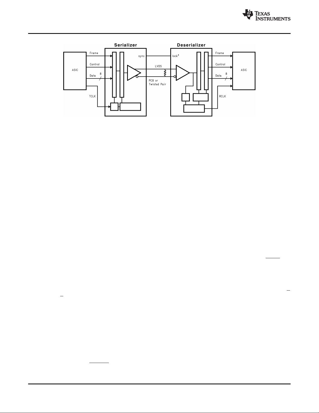
The DS92LV1021A transforms a 10-bit wide parallel
2
• Specified Transition Every Data Transfer Cycle
LVCMOS/LVTTL data bus into a single high speed
• Single Differential Pair Eliminates Multi-
Bus LVDS serial data stream with embedded clock.
Channel Skew
The DS92LV1021A can transmit data over
• Flow-Through Pinout for Easy PCB Layout
backplanes or cable. The single differential pair data
path makes PCB design easier. In addition, the
• 400 Mbps Serial Bus LVDS Bandwidth (at 40
reduced cable, PCB trace count, and connector size
MHz Clock)
tremendously reduce cost. Since one output transmits
• 10-bit Parallel Interface for 1 Byte Data Plus 2
both clock and data bits serially, it eliminates clock-to-
Control Bits
data and data-to-data skew. The powerdown pin
saves power by reducing supply current when the
• Programmable Edge Trigger on Clock
device is not being used. Upon power up of the
• Bus LVDS Serial Output Rated for 27Ω Load
Serializer, you can choose to activate synchronization
• Small 28-Lead SSOP Package-DB
mode or use one of TI’s Deserializers in the
synchronization-to-random-data feature. By using the
synchronization mode, the Deserializer will establish
lock to a signal within specified lock times. In
addition, the embedded clock specifies a transition on
the bus every 12-bit cycle. This eliminates
transmission errors due to charged cable conditions.
Furthermore, you may put the DS92LV1021A output
pins into TRI-STATE to achieve a high impedance
state. The PLL can lock to frequencies between 16
MHz and 40 MHz.
Block Diagram
1
Please be aware that an important notice concerning availability, standard warranty, and use in critical applications of
Texas Instruments semiconductor products and disclaimers thereto appears at the end of this data sheet.
2All trademarks are the property of their respective owners.
PRODUCTION DATA information is current as of publication date.
Copyright © 2002–2013, Texas Instruments Incorporated
Products conform to specifications per the terms of the Texas
Instruments standard warranty. Production processing does not
necessarily include testing of all parameters.
DS92LV1021A
SNLS151G –OCTOBER 2002–REVISED APRIL 2013
www.ti.com
Functional Description
The DS92LV1021A is an upgrade to the DS92LV1021. The DS92LV1021A no longer has a power-up sequence
requirement. Like the DS92LV1021, the DS92LV1021A is a 10-bit Serializer designed to transmit data over a
differential backplane at clock speeds from 16 to 40MHz. It may also be used to drive data over Unshielded
Twisted Pair (UTP) cable.
The DS92LV1021A can be used with any of TI’s 10-bit BLVDS Deserializers (DS92LV1212A for example) and
has three active states of operation: Initialization, Data Transfer, and Resynchronization; and two passive states:
Powerdown and TRI-STATE.
The following sections describe each active and passive state.
Initialization
Before data can be transferred, the Serializer must be initialized. Initialization refers to synchronization of the
Serializer’s PLL to a local clock.
When V
CC
is applied to the Serializer, the outputs are held in TRI-STATE and internal circuitry is disabled by on-
chip power-on circuitry. When V
CC
reaches V
CC
OK (2.5V) the Serializer’s PLL begins locking to the local clock.
The local clock is the transmit clock, TCLK, provided by the source ASIC or other device.
Once the PLL locks to the local clock, the Serializer is ready to send data or SYNC patterns, depending on the
levels of the SYNC1 and SYNC2 inputs. The SYNC pattern is composed of six ones and six zeros switching at
the input clock rate.
Control of the SYNC pins is left to the user. One recommendation is a direct feedback loop from the LOCK pin.
Under all circumstances, the Serializer stops sending SYNC patterns after both SYNC inputs return low.
Data Transfer
After initialization, the Serializer inputs DIN0–DIN9 may be used to input data to the Serializer. Data is clocked
into the Serializer by the TCLK input. The edge of TCLK used to strobe the data is selectable via the TCLK_R/F
pin. TCLK_R/F high selects the rising edge for clocking data and low selects the falling edge. If either of the
SYNC inputs is high for 5*TCLK cycles, the data at DIN0-DIN9 is ignored regardless of the clock edge.
A start bit and a stop bit, appended internally, frame the data bits in the register. The start bit is always high and
the stop bit is always low. The start and stop bits function as the embedded clock bits in the serial stream.
Serialized data and clock bits (10+2 bits) are transmitted from the serial data output (DO±) at 12 times the TCLK
frequency. For example, if TCLK is 40 MHz, the serial rate is 40 × 12 = 480 Mega bits per second. Since only 10
bits are from input data, the serial “payload” rate is ten times the TCLK frequency. For instance, if TCLK = 40
MHz, the payload data rate is 40 × 10 = 400 Mbps. TCLK is provided by the data source and must be in the
range of 16 MHz to 40 MHz nominal.
The outputs (DO±) can drive a backplane or a point-to-point connection. The outputs transmit data when the
enable pin (DEN) is high, PWRDN is high, and SYNC1 and SYNC2 are low. The DEN pin may be used to TRI-
STATE the outputs when driven low.
2 Submit Documentation Feedback Copyright © 2002–2013, Texas Instruments Incorporated
Product Folder Links: DS92LV1021A
DS92LV1021A
www.ti.com
SNLS151G –OCTOBER 2002–REVISED APRIL 2013
Ideal Crossing Point
The ideal crossing point is the best case start and stop point for a normalized bit. Each ideal crossing point is
found by dividing the clock period by twelve--two clock bits plus ten data bits. For example, a 40 MHz clock has a
period of 25ns. The 25ns divided by 12 bits is approximately 2.08ns. This means that each bit width is
approximately 2.08ns, and the ideal crossing points occur every 2.08ns. For a graphical representation, please
see Figure 9.
Resynchronization
The Deserializer LOCK pin driven low indicates that the Deserializer PLL is locked to the embedded clock edge.
If the Deserializer loses lock, the LOCK output will go high and the outputs (including RCLK) will be TRI-STATE.
The LOCK pin must be monitored by the system to detect a loss of synchronization, and the system must decide
if it is necessary to pulse the Serializer SYNC1 or SYNC2 pin to resynchronize. There are multiple approaches
possible. One recommendation is to provide a feedback loop using the LOCK pin itself to control the sync
request of the Serializer (SYNC1 or SYNC2). At the time of publication, other than the DS92LV1210, all other
Deserializers from TI have random lock capability. This feature does not require the system user to send SYNC
patterns upon loss of lock. However, lock times can only be specified with transmission of SYNC patterns. Dual
SYNC pins are provided for multiple control in a multi-drop application.
Powerdown
The Powerdown state is a low power sleep mode that the Serializer and Deserializer may use to reduce power
when no data is being transferred. The device enters Powerdown when the PWRDN pin is driven low on the
Serializer. In Powerdown, the PLL stops and the outputs go into TRI-STATE, disabling load current and reducing
supply current into the milliamp range. To exit Powerdown, PWRDN must be driven high.
Both the Serializer and Deserializer must reinitialize and resynchronize before data can be transferred. The
Deserializer will initialize and assert LOCK high until it is locked to the Bus LVDS clock.
TRI-STATE
For the Serializer, TRI-STATE is entered when the DEN pin is driven low. This will TRI-STATE both driver output
pins (DO+ and DO−). When DEN is driven high, the serializer will return to the previous state as long as all other
control pins remain static (SYNC1, SYNC2, PWRDN, TCLK_R/F).
These devices have limited built-in ESD protection. The leads should be shorted together or the device placed in conductive foam
during storage or handling to prevent electrostatic damage to the MOS gates.
Absolute Maximum Ratings
(1)(2)
Supply Voltage (V
CC
) −0.3V to +4V
CMOS/TTL Input Voltage −0.3V to (V
CC
+0.3V)
CMOS/TTL Output Voltage −0.3V to (V
CC
+0.3V)
Bus LVDS Receiver Input Voltage −0.3V to +3.9V
Bus LVDS Driver Output Voltage −0.3V to +3.9V
Bus LVDS Output Short Circuit Duration Continuous
Junction Temperature +150°C
Storage Temperature −65°C to +150°C
Lead Temperature (Soldering, 4 seconds) +260°C
Maximum Package Power Dissipation Capacity @ 25°C Package:
28L SSOP 1.27 W
Package Derating: 28L SSOP 10.2 mW/°C above +25°C
ESD Rating (HBM)
(3)
>2.0kV
(1) “Absolute Maximum Ratings” are those values beyond which the safety of the device cannot be specified. They are not meant to imply
that the devices should be operated at these limits. The table of “Electrical Characteristics” specifies conditions of device operation.
(2) If Military/Aerospace specified devices are required, please contact the TI Sales Office/ Distributors for availability and specifications.
(3) With a limited Engineering sample size, ESD (HBM) testing passed 2.5kV
Copyright © 2002–2013, Texas Instruments Incorporated Submit Documentation Feedback 3
Product Folder Links: DS92LV1021A
DS92LV1021A
SNLS151G –OCTOBER 2002–REVISED APRIL 2013
www.ti.com
Recommended Operating Conditions
Min Nom Max Units
Supply Voltage (V
CC
) 3.0 3.3 3.6 V
Operating Free Air Temperature (T
A
) −40 +25 +85 °C
Supply Noise Voltage (V
CC
) 100 mV
P-P
Electrical Characteristics
Over recommended operating supply and temperature ranges unless otherwise specified.
(1)(2)
Symbol Parameter Conditions Min Typ Max Units
SERIALIZER CMOS/TTL DC SPECIFICATIONS (apply to DIN0-9, TCLK, PWRDN, TCLK_R/F, SYNC1, SYNC2, DEN)
V
IH
High Level Input Voltage 2.0 V
CC
V
V
IL
Low Level Input Voltage GND 0.8 V
V
CL
Input Clamp Voltage I
CL
= −18 mA −1.5 V
I
IN
Input Current V
IN
= 0V or 3.6V −10 ±2 +10 μA
SERIALIZER Bus LVDS DC SPECIFICATIONS (apply to pins DO+ and DO−)
V
OD
Output Differential Voltage
200 270 mV
(DO+)–(DO−)
ΔV
OD
Output Differential Voltage
35 mV
RL = 27Ω
Unbalance
V
OS
Offset Voltage 0.78 1.1 1.3 V
ΔV
OS
Offset Voltage Unbalance 35 mV
I
OS
Output Short Circuit Current D0 = 0V, DIN = High,PWRDN and DEN = 2.4V −30 −40 mA
I
OZ
TRI-STATE Output Current PWRDN or DEN = 0.8V, DO = 0V or VCC −10 ±1 +10 μA
I
OX
Power-Off Output Current VCC = 0V, DO = 0V or VCC −20 ±1 +20 μA
SERIALIZER SUPPLY CURRENT (apply to pins DVCC and AVCC)
I
CCD
f = 40 MHz 40 55 mA
Worst Case Serializer Supply
RL = 27Ω, Figure 1
Current
f = 16 MHz 28 35 mA
I
CCXD
Serializer Supply Current
PWRDN = 0.8V 88 300 μA
Powerdown
(1) Typical values are given for V
CC
= 3.3V and T
A
= +25°C.
(2) Current into device pins is defined as positive. Current out of device pins is defined as negative. Voltages are referenced to ground
except VOD, ΔVOD, VTH and VTL which are differential voltages.
Serializer Timing Requirements for TCLK
Over recommended operating supply and temperature ranges unless otherwise specified.
(1)(2)
Symbol Parameter Conditions Min Typ Max Units
t
TCP
Transmit Clock Period 25 T 62.5 ns
t
TCIH
Transmit Clock High Time 0.4T 0.5T 0.6T ns
t
TCIL
Transmit Clock Low Time 0.4T 0.5T 0.6T ns
t
CLKT
TCLK Input Transition Time 3 6 ns
t
JIT
TCLK Input Jitter ps
150
(RMS)
(1) Typical values are given for V
CC
= 3.3V and T
A
= +25°C.
(2) Current into device pins is defined as positive. Current out of device pins is defined as negative. Voltages are referenced to ground
except VOD, ΔVOD, VTH and VTL which are differential voltages.
4 Submit Documentation Feedback Copyright © 2002–2013, Texas Instruments Incorporated
Product Folder Links: DS92LV1021A
剩余17页未读,继续阅读
资源评论
不觉明了
- 粉丝: 3248
- 资源: 5614
上传资源 快速赚钱
- 我的内容管理 展开
- 我的资源 快来上传第一个资源
- 我的收益 登录查看自己的收益
- 我的积分 登录查看自己的积分
- 我的C币 登录后查看C币余额
- 我的收藏
- 我的下载
- 下载帮助
最新资源
- Windows平台下的实用应用软件集
- 迅雷_8.01.0.9024.apk
- 基于Python基于pygame库开发的飞机大战射击游戏,在游戏中,玩家控制一架飞船,在太空中射击飞行的小行星以获得分数
- 基于python 实现多模态的动态用户属性挖掘系统
- 窗体动态视觉呈现效果或窗体动画化展示效果
- 本资源包涵盖了丰富的设计辅助功能,包括标注、文本编辑、路径操作、颜色管理、画板调整、包装设计、拼版、设计优化、输出设置和效果处理
- 城市鎏金风素材PPT.pptx
- 305建筑结构水电欧式6套(14.5x20.2)\施工图\C型施工图\水1TJ-卫生间大样031020.dwg
- business鎏金风格.pptx
- 305建筑结构水电欧式6套(14.5x20.2)\施工图\C型施工图\水1-C型平面031014.dwg
资源上传下载、课程学习等过程中有任何疑问或建议,欢迎提出宝贵意见哦~我们会及时处理!
点击此处反馈
安全验证
文档复制为VIP权益,开通VIP直接复制
信息提交成功