没有合适的资源?快使用搜索试试~ 我知道了~
TI-DS92LV18.pdf
![star](https://csdnimg.cn/release/downloadcmsfe/public/img/star.98a08eaa.png)
温馨提示
![preview](https://dl-preview.csdnimg.cn/87429807/0001-79bbbcc833a8700e0a1689cbe10ab98e_thumbnail.jpeg)
![preview-icon](https://csdnimg.cn/release/downloadcmsfe/public/img/scale.ab9e0183.png)
试读
26页
LVDS解串器
资源推荐
资源详情
资源评论
![](https://csdnimg.cn/release/download_crawler_static/87429807/bg1.jpg)
DS92LV18
www.ti.com
SNLS156E –SEPTEMBER 2003–REVISED APRIL 2013
DS92LV18 18-Bit Bus LVDS Serializer/Deserializer - 15-66 MHz
Check for Samples: DS92LV18
1
FEATURES
DESCRIPTION
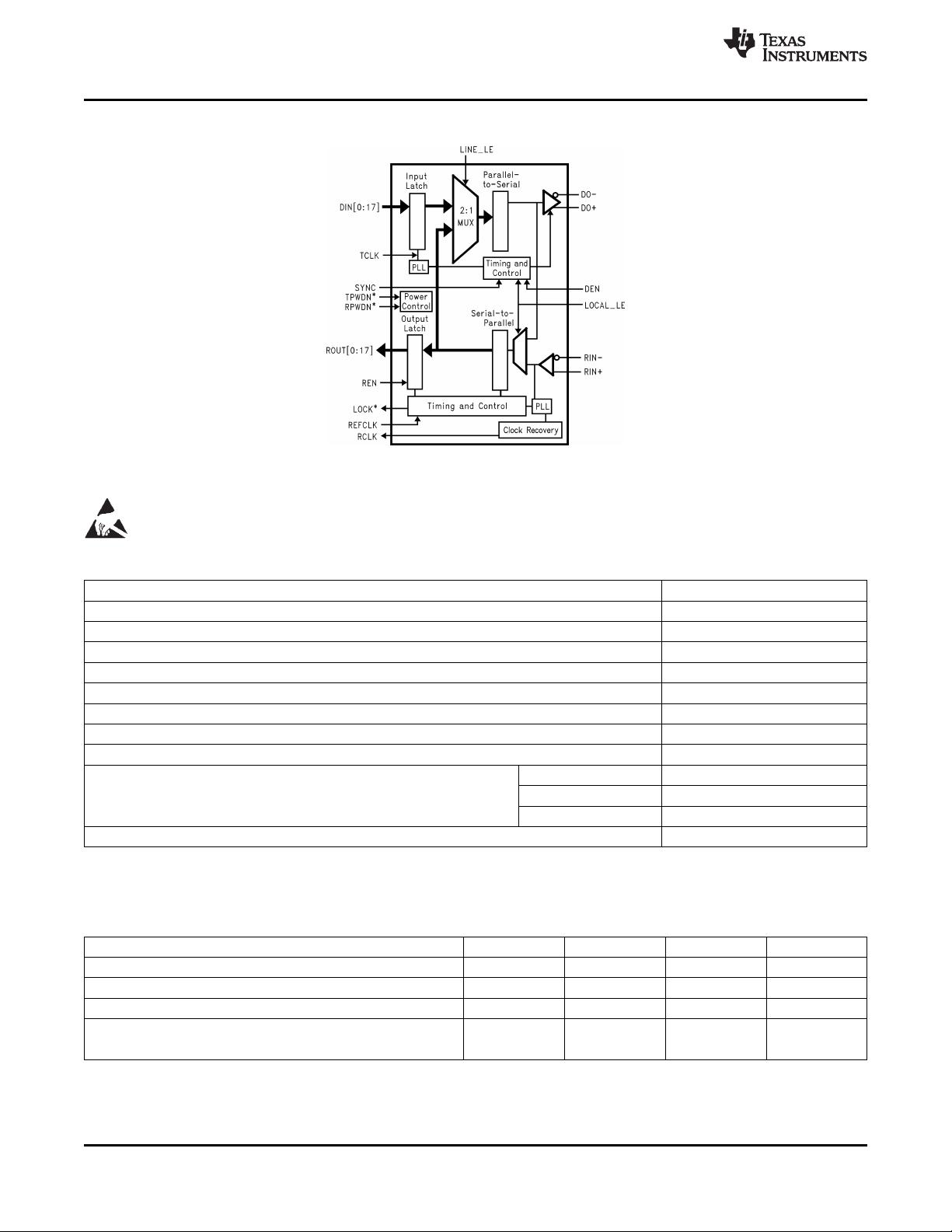
The DS92LV18 Serializer/Deserializer (SERDES) pair
2
• 15–66 MHz 18:1/1:18 Serializer/Deserializer
transparently translates a 18–bit parallel bus into a
(2.376 Gbps Full Duplex Throughput)
BLVDS serial stream with embedded clock
• Independent Transmitter and Receiver
information. This single serial stream simplifies
Operation with Separate Clock, Enable, and
transferring a 18-bit, or less, bus over PCB traces
Power Down Pins
and cables by eliminating the skew problems
between parallel data and clock paths. It saves
• Hot Plug Protection (Power Up High
system cost by narrowing data paths that in turn
Impedance) and Synchronization (Receiver
reduce PCB layers, cable width, and connector size
Locks to Random Data)
and pins.
• Wide ±5% Reference Clock Frequency
This SERDES pair includes built-in system and
Tolerance for Easy System Design Using
device test capability. The line loopback feature
Locally-Generated Clocks
enables the user to check the integrity of the serial
• Line and Local Loopback Modes
data transmission paths of the transmitter and
• Robust BLVDS Serial Transmission Across
receiver while deserializing the serial data to parallel
Backplanes and Cables for Low EMI
data at the receiver outputs. The local loopback
feature enables the user to check the integrity of the
• No External Coding Required
transceiver from the local parallel-bus side.
• Internal PLL, No External PLL Components
The DS92LV18 incorporates modified BLVDS
Required
signaling on the high-speed I/O. BLVDS provides a
• Single +3.3V Power Supply
low power and low noise environment for reliably
• Low Power: 90mA (typ) Transmitter, 100mA
transferring data over a serial transmission path. The
(typ) at 66 MHz with PRBS-15 Pattern
equal and opposite currents through the differential
data path control EMI by coupling the resulting
• ±100 mV Receiver Input Threshold
fringing fields together.
• Loss of Lock Detection and Reporting Pin
• Industrial −40 to +85°C Temperature Range
• >2.0kV HBM ESD
• Compact, Standard 80-Pin LQFP Package
1
Please be aware that an important notice concerning availability, standard warranty, and use in critical applications of
Texas Instruments semiconductor products and disclaimers thereto appears at the end of this data sheet.
2All trademarks are the property of their respective owners.
PRODUCTION DATA information is current as of publication date.
Copyright © 2003–2013, Texas Instruments Incorporated
Products conform to specifications per the terms of the Texas
Instruments standard warranty. Production processing does not
necessarily include testing of all parameters.
![](https://csdnimg.cn/release/download_crawler_static/87429807/bg2.jpg)
DS92LV18
SNLS156E –SEPTEMBER 2003–REVISED APRIL 2013
www.ti.com
Block Diagram
Figure 1. DS92LV18
These devices have limited built-in ESD protection. The leads should be shorted together or the device placed in conductive foam
during storage or handling to prevent electrostatic damage to the MOS gates.
Absolute Maximum Ratings
(1)(2)
Supply Voltage (V
CC
) −0.3V to +4V
LVCMOS/LVTTL Input Voltage −0.3V to (V
CC
+0.3V)
LVCMOS/LVTTL Output Voltage −0.3V to (V
CC
+0.3V)
Bus LVDS Receiver Input Voltage −0.3V to +3.9V
Bus LVDS Driver Output Voltage −0.3V to +3.9V
Bus LVDS Output Short Circuit Duration 10ms
Junction Temperature +150°C
Storage Temperature −65°C to +150°C
Lead Temperature (Soldering, 4 seconds) +260°C
Maximum Package Power Dissipation Capacity Package Derating: 80L LQFP 23.2 mW/°C above +25°C
θ
JA
43°C/W
θ
JC
11.1°C/W
ESD Rating (HBM) >2.0kV
(1) “Absolute Maximum Ratings” are those values beyond which the safety of the device cannot be ensured. They are not meant to imply
that the devices should be operated at these limits. The table of “Electrical Characteristics” specifies conditions of device operation.
(2) If Military/Aerospace specified devices are required, please contact the TI Sales Office/Distributors for availability and specifications.
Recommended Operating Conditions
Min Nom Max Units
Supply Voltage (V
CC
) 3.15 3.3 3.45 V
Operating Free Air Temperature (T
A
) −40 +25 +85 °C
Clock Rate 15 66 MHz
Supply Noise 100 mV
(p-p)
2 Submit Documentation Feedback Copyright © 2003–2013, Texas Instruments Incorporated
Product Folder Links: DS92LV18
![](https://csdnimg.cn/release/download_crawler_static/87429807/bg3.jpg)
DS92LV18
www.ti.com
SNLS156E –SEPTEMBER 2003–REVISED APRIL 2013
Electrical Characteristics
Over recommended operating supply and temperature ranges unless otherwise specified.
Symbol Parameter Conditions Pin/Freq. Min Typ
(1)
Max Units
LVCMOS/LVTTL DC Specifications
V
IH
High Level Input Voltage 2.0 V
CC
V
DEN, TCLK, TPWDN,
DIN,
V
IL
Low Level Input Voltage GND 0.8 V
SYNC, RCLK_R/F,
V
CL
Input Clamp Voltage I
CL
= −18 mA -0.7 −1.5 V
REN, REFCLK,
RPWDN
I
IN
Input Current V
IN
= 0V or 3.6V −10 ±2 +10 μA
V
OH
High Level Output Voltage I
OH
= −9 mA 2.3 3.0 V
CC
V
V
OL
Low Level Output Voltage I
OL
= 9 mA R
OUT
, RCLK, LOCK GND 0.33 0.5 V
I
OS
Output Short Circuit Current VOUT = 0V −15 −48 −85 mA
PWRDN or REN =
I
OZ
TRI-STATE Output Current 0.8V, V
OUT
= 0V or R
OUT
, RCLK −10 ±0.4 +10 μA
VCC
Bus LVDS DC specifications
Differential Threshold High
VTH
(2)
+100 mV
Voltage
VCM = +1.1V
Differential Threshold Low
VTL
(2)
−100 mV
Voltage
RI+, RI-
V
IN
= +2.4V, V
CC
=
−10 ±5 +10 μA
3.6V or 0V
I
IN
Input Current
V
IN
= 0V, V
CC
= 3.6V or
−10 ±5 +10 μA
0V
Output Differential Voltage Figure 19,
(3)
,
V
OD
(2)
350 500 550 mV
(DO+) - (DO-) R
L
= 100Ω
Output Differential Voltage
ΔV
OD
(2)
2 15 mV
Unbalance
V
OS
Offset Voltage 1.05 1.2 1.25 V
ΔV
OS
Offset Voltage Unbalance 2.7 15 mV
DO = 0V, Din = H,
DO+, DO-
I
OS
Output Short Circuit Current TPWDN and DEN = -35 -50 -70 mA
2.4V
TPWDN or DEN =
I
OZ
TRI-STATE Output Current 0.8V, DO = 0V OR -10 ± 1 10 µA
VDD
VDD = 0V, DO = 0V or
I
OX
Power-Off Output Current -10 ± 1 10 µA
3.6V
SER/DES SUPPLY CURRENT (DVDD, PVDD and AVDD pins)
C
L
= 15pF, f = 66 MHz, PRBS-15
190 mA
R
L
= 100 Ω pattern
Total Supply Current (includes
I
CCT
f = 66 MHz, Worst case
load current)
C
L
= 15 pF,
pattern (Checker-board 220 320 mA
R
L
= 100 Ω
pattern)
PWRDN = 0.8V, REN
I
CCX
Supply Current Powerdown 1.5 3.0 mA
= 0.8V
(1) Typical values are given for V
CC
= 3.3V and T
A
= +25°C.
(2) Current into device pins is defined as positive. Current out of device pins is defined as negative. Voltages are referenced to ground
except VOD, ΔVOD, VTH and VTL which are differential voltages.
(3) The VOD specification is a measurement of the difference between the single-ended VOH and VOL output voltages across a100 ohm
load. Applying the formula OUT+ - OUT- to the differential outputs will result in a waveform with peak to peak amplitude equal to twice
the datasheet indicated VOD.
Copyright © 2003–2013, Texas Instruments Incorporated Submit Documentation Feedback 3
Product Folder Links: DS92LV18
![](https://csdnimg.cn/release/download_crawler_static/87429807/bg4.jpg)
DS92LV18
SNLS156E –SEPTEMBER 2003–REVISED APRIL 2013
www.ti.com
Serializer Timing Requirements for TCLK
Over recommended operating supply and temperature ranges unless otherwise specified.
Symbol Parameter Conditions Min Typ Max Units
t
TCP
Transmit Clock Period 15.2 T 66.7 ns
t
TCIH
Transmit Clock High Time 0.4T 0.5T 0.6T ns
t
TCIL
Transmit Clock Low Time 0.4T 0.5T 0.6T ns
t
CLKT
TCLK Input Transition Time 3 6 ns
ps
t
JIT
TCLK Input Jitter See
(1)
80
(RMS)
(1) Specified by Design (SBD) using statistical analysis.
Serializer Switching Characteristics
Over recommended operating supply and temperature ranges unless otherwise specified.
Symbol Parameter Conditions Min Typ Max Units
Bus LVDS Low-to-High
t
LLHT
0.2 0.4 ns
Figure 4,
(1)
Transition Time
R
L
= 100Ω,
Bus LVDS High-to-Low
C
L
=10pF to GND
t
LHLT
0.2 0.4 ns
Transition Time
t
DIS
DIN (0-17) Setup to TCLK Figure 7,
(1)
2.4 ns
R
L
= 100Ω,
t
DIH
DIN (0-17) Hold from TCLK 0 ns
C
L
=10pF to GND
DO ± HIGH to
t
HZD
2.3 10 ns
TRI-STATE Delay
DO ± LOW to TRI-STATE
t
LZD
1.9 10 ns
Delay
Figure 8
(2)
R
L
= 100Ω,
C
L
=10pF to GND
DO ± TRI-STATE to HIGH
t
ZHD
1.0 10 ns
Delay
DO ± TRI-STATE to LOW
t
ZLD
1.0 10 ns
Delay
t
SPW
SYNC Pulse Width Figure 10, R
L
= 100Ω 5*t
TCP
6*t
TCP
ns
t
PLD
Serializer PLL Lock Time Figure 9, R
L
= 100Ω 510*t
TCP
1024*t
TCP
ns
t
SD
Serializer Delay Figure 11, R
L
= 100Ω t
TCP
+ 1.0 t
TCP
+ 2.0 t
TCP
+ 4.0 ns
Room Temp., 3.3V, ps
t
RJIT
Random Jitter 4.5
66 MHz (RMS)
15 MHz -430 190 ps
Deterministic Jitter
t
DJIT
Figure 17,
(1)
66 MHz -40 70 ps
(1) Specified by Design (SBD) using statistical analysis.
(2) Due to TRI-STATE of the Serializer, the Deserializer will lose PLL lock and have to resynchronize before data transfer.
Deserializer Timing Requirements for REFCLK
Over recommended operating supply and temperature ranges unless otherwise specified.
Symbol Parameter Conditions Min Typ Max Units
t
RFCP
REFCLK Period 15.2 T 66.7 ns
t
RFDC
REFCLK Duty Cycle 40 50 60 %
t
RFCP
/ t
TCP
Ratio of REFCLK to TCLK 0.95 1.05
t
RFTT
REFCLK Transition Time 6 ns
4 Submit Documentation Feedback Copyright © 2003–2013, Texas Instruments Incorporated
Product Folder Links: DS92LV18
![](https://csdnimg.cn/release/download_crawler_static/87429807/bg5.jpg)
DS92LV18
www.ti.com
SNLS156E –SEPTEMBER 2003–REVISED APRIL 2013
Deserializer Switching Characteristics
Over recommended operating supply and temperature ranges unless otherwise specified.
Symbol Parameter Conditions Pin/Freq. Min Typ Max Units
Receiver out Clock
t
RCP
t
RCP
= t
TCP
RCLK 15.2 66.7 ns
Period
t
RDC
RCLK Duty Cycle RCLK 45 50 55 %
CMOS/TTL Low-to-
t
CLH
2.2 4 ns
High Transition Time
CL = 15 pF
Figure 5
CMOS/TTL High-to-
t
CHL
2.2 4 ns
ROUT(0-17),
Low Transition Time
LOCK,
ROUT (0-9) Setup
RCLK
t
ROS
0.35*t
RCP
0.5*t
RCP
ns
Data to RCLK
Figure 13
ROUT (0-9) Hold
t
ROH
−0.35*t
RCP
−0.5*t
RCP
ns
Data to RCLK
HIGH to TRI-STATE
t
HZR
2.2 10 ns
Delay
LOW to TRI-STATE
t
LZR
2.2 10 ns
Delay
ROUT(0-17),
Figure 14
LOCK
TRI-STATE to HIGH
t
ZHR
2.3 10 ns
Delay
TRI-STATE to LOW
t
ZLR
2.9 10 ns
Delay
t
DD
Deserializer Delay RCLK 1.75*t
RCP
+ 2.1 1.75*t
RCP
+ 4.0 1.75*t
RCP
+ 6.1 ns
Deserializer PLL 15MHz 3.7 10 μs
Lock Time from Figure 15,
t
DSR1
(1)
Powerdown (with
(2)(3)
66 MHz 1.9 4 μs
SYNCPAT)
Deserializer PLL 15MHz 1.5 5 μs
Figure 16,
t
DSR2
(1)
Lock time from
(2)(3)
66 MHz 0.9 2 μs
SYNCPAT
15 MHz 1490 ps
Ideal Deserializer Figure 18
t
RNMI-R
Noise Margin Right
(4)(3)
66 MHz 180 ps
15 MHz 1460 ps
Ideal Deserializer Figure 18
t
RNMI-L
Noise Margin Left
(4)(3)
66 MHz 330 ps
15 MHz 1060 ps
Total Interconnect
t
JI
See
(5)
Jitter Budget
66 MHz 160 ps
(1) t
DSR1
is the time required by the deserializer to obtain lock when exiting powerdown mode. t
DSR1
is specified with synchronization
patterns (SYNCPATs) present at the LVDS inputs (RI+ and RI-) before exiting powerdown mode. t
DSR2
is the time required to obtain
lock for the powered-up and enabled deserializer when the LVDS input (RI+ and RI-) conditions change from not receiving data to
receiving synchronization patterns. Both t
DSR1
and t
DSR2
are specified with the REFCLK running and stable.
(2) A sync pattern is a fixed pattern with 9-bits of data high followed by 9-bits of data low. The SYNC pattern is automatically generated by
the transmitter when the SYNC pin is pulled high.
(3) Specified by Design (SBD) using statistical analysis.
(4) t
RNMI
is a measure of how much phase noise (jitter) the deserializer can tolerate in the incoming data stream before bit errors occur. It is
a measurement in reference with the ideal bit position, please see AN-1217 (SNLA053) for detail.
(5) Total Interconnect Jitter Budget (t
JI
) specifies the allowable jitter added by the interconnect assuming both transmitter and receiver are
DS92LV18 circuits. t
JI
is GBD using statistical analysis.
Copyright © 2003–2013, Texas Instruments Incorporated Submit Documentation Feedback 5
Product Folder Links: DS92LV18
剩余25页未读,继续阅读
资源评论
![avatar-default](https://csdnimg.cn/release/downloadcmsfe/public/img/lazyLogo2.1882d7f4.png)
- m0_745259962023-02-15#完美解决问题 #运行顺畅 #内容详尽 #全网独家 #注释完整
- CSDN_1872023-02-15#完美解决问题 #运行顺畅 #内容详尽 #全网独家 #注释完整
- 2301_763960562023-02-15#完美解决问题 #运行顺畅 #内容详尽 #全网独家 #注释完整
![avatar](https://profile-avatar.csdnimg.cn/107303f5121d47e49d12d0a9ae68af10_weixin_54787054.jpg!1)
不觉明了
- 粉丝: 3234
- 资源: 5614
上传资源 快速赚钱
我的内容管理 展开
我的资源 快来上传第一个资源
我的收益
登录查看自己的收益我的积分 登录查看自己的积分
我的C币 登录后查看C币余额
我的收藏
我的下载
下载帮助
![voice](https://csdnimg.cn/release/downloadcmsfe/public/img/voice.245cc511.png)
![center-task](https://csdnimg.cn/release/downloadcmsfe/public/img/center-task.c2eda91a.png)
最新资源
- 数据库管理工具:dbeaver-ce-23.1.3-amd64.deb
- 数据库管理工具:dbeaver-ce-23.1.2-amd64.deb
- 数据库管理工具:dbeaver-ce-23.1.1-amd64.deb
- 基于SRM频谱模型的粗糙表面仿真
- 数据库管理工具:dbeaver-ce-23.1.0-amd64.deb
- 数据库管理工具:dbeaver-ce-23.0.4-amd64.deb
- nginx-deploy.yaml
- 编程项目实战:基于ASP.NET架构的学生信息管理系统(含源代码+毕设文档)
- 毕设项目:学生信息管理系统(asp.net+源代码+文档)
- 腾讯研究院2024向AI而行共筑新质生产力-行业大模型调研报告
资源上传下载、课程学习等过程中有任何疑问或建议,欢迎提出宝贵意见哦~我们会及时处理!
点击此处反馈
![feedback](https://img-home.csdnimg.cn/images/20220527035711.png)
![feedback-tip](https://img-home.csdnimg.cn/images/20220527035111.png)
安全验证
文档复制为VIP权益,开通VIP直接复制
![dialog-icon](https://csdnimg.cn/release/downloadcmsfe/public/img/green-success.6a4acb44.png)