没有合适的资源?快使用搜索试试~ 我知道了~
TI-DS92LV1260.pdf
![star](https://csdnimg.cn/release/downloadcmsfe/public/img/star.98a08eaa.png)
温馨提示
![preview](https://dl-preview.csdnimg.cn/87432242/0001-153a8c26318873f82a67d4e6e717fcb3_thumbnail.jpeg)
![preview-icon](https://csdnimg.cn/release/downloadcmsfe/public/img/scale.ab9e0183.png)
试读
20页
串并转换器
资源推荐
资源详情
资源评论
![](https://csdnimg.cn/release/download_crawler_static/87432242/bg1.jpg)
DS92LV1260
www.ti.com
SNLS134F –DECEMBER 2000–REVISED APRIL 2013
DS92LV1260 Six Channel 10 Bit BLVDS Deserializer
Check for Samples: DS92LV1260
1
FEATURES
DESCRIPTION
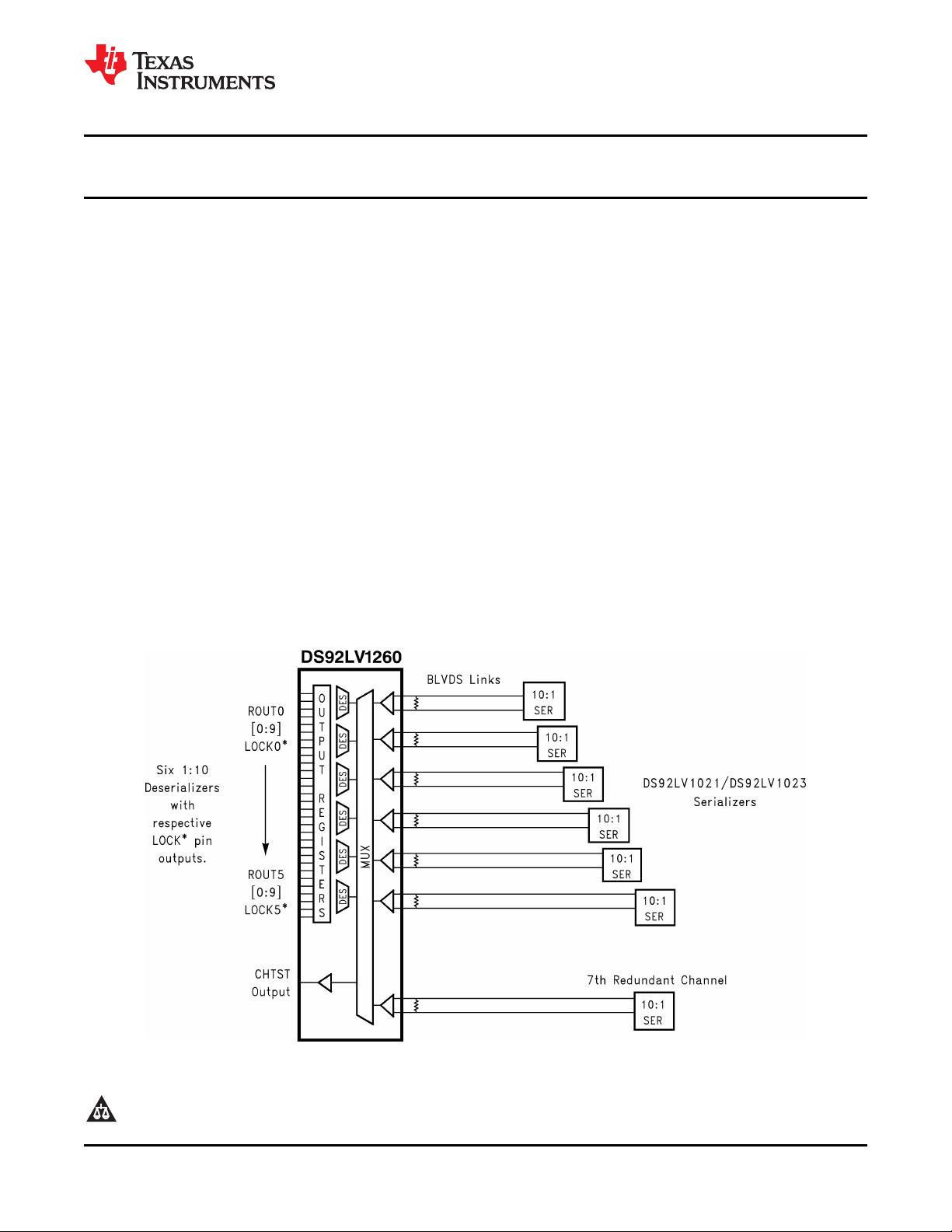
The DS92LV1260 integrates six deserializer devices
2
• Deserializes One to Six BusLVDS Input Serial
into a single chip. The chip uses a 0.25u CMOS
Data Streams with Embedded Clocks
process technology. The DS92LV1260 can
• Seven Selectable Serial Inputs to Support n+1
simultaneously deserialize up to six data streams that
Redundancy of Deserialized Streams
have been serialized by the Texas Instruments
DS92LV1021 or DS92LV1023 Bus LVDS serializers.
• Seventh Channel has Single Pin Monitor
The device also includes a seventh serial input
Output That Reflects Input From Seventh
channel that serves as a redundant input.
Channel Input
• Parallel Clock Rate up to 40MHz Each deserializer block in the DS92LV1260 operates
independently with its own clock recovery circuitry
• On Chip Filtering for PLL
and lock-detect signaling.
• Absolute Maximum Worst Case Power
The DS92LV1260 uses a single +3.3V power supply
Dissipation = 1.9W at 3.6V
with a typical power dissipation of 1.2W at 3.3V with
• High Impedance Inputs Upon Power Off (V
cc
=
a PRBS-15 pattern. Refer to the Connection
0V)
Diagrams for packaging information.
• Single Power Supply at +3.3V
• 196-pin NFBGA Package (Low-profile Ball Grid
Array) Package
• Industrial Temperature Range Operation:
−40°C to +85°C
Block Diagram
Figure 1. Application
1
Please be aware that an important notice concerning availability, standard warranty, and use in critical applications of
Texas Instruments semiconductor products and disclaimers thereto appears at the end of this data sheet.
2All trademarks are the property of their respective owners.
PRODUCTION DATA information is current as of publication date.
Copyright © 2000–2013, Texas Instruments Incorporated
Products conform to specifications per the terms of the Texas
Instruments standard warranty. Production processing does not
necessarily include testing of all parameters.
![](https://csdnimg.cn/release/download_crawler_static/87432242/bg2.jpg)
DS92LV1260
SNLS134F –DECEMBER 2000–REVISED APRIL 2013
www.ti.com
These devices have limited built-in ESD protection. The leads should be shorted together or the device placed in conductive foam
during storage or handling to prevent electrostatic damage to the MOS gates.
Absolute Maximum Ratings
(1)(2)
Supply Voltage (V
cc
) -0.3 to 4V
Bus LVDS Input Voltage (Rin +/-) -0.3V to 3.9V
Maximum Package Power Dissipation @25°C 3.7W
Package Thermal Resistance
θ
JA
196 NFBGA: 34°C/W
θ
JC
196 NFBGA: 8°C/W
Storage Temp. Range -65°C to +150°C
Junction Termperature +150°C
Lead Temperature (Soldering 10 Sec) +225°C
ESD Rating:
Human Body Model >3KV
Machine Model >750V
Reliability Information
Transistor Count 35,682
(1) “Absolute Maximum Ratings” are those values beyond which the safety of the device cannot be specified. They are not meant to imply
that the devices should be operated at these limits. The table of “Electrical Characteristics” specifies conditions of device operation.
(2) If Military/Aerospace specified devices are required, please contact the TI Sales Office/ Distributors for availability and specifications.
Recommended Operating Conditions
Supply Voltage (V
CC
) 3.0V to 3.6V
Operating Free Air -40°C to +85°C
Temperature (T
A
)
Operating Frequency 16-40 MHz
Electrical Characteristics
(1)
Basic functionality and specifications per deserializer channel will be similar to DS92LV1212A. Over recommended operating
supply and termperature ranges unless otherwise specified.
(2)
Parameter Test Conditions Pin/Freq. Min Typ Max Units
LVCMOS/LVTTL DC Specifications:
V
IH
High Level Input Voltage 2.0 V
CC
V
V
IL
Low Level Input Voltage GND 0.8 V
REN,REFCLK,PWRDWN,
SEL (0:2),R
OUT
V
CL
Input Clamp Voltage -0.87 -1.5 V
I
IN
Input Current V
in
= 0 or 3.6V -10 +10 uA
V
OH
High Level Output Voltage I
OH
= -6mA 2 3 V
CC
V
V
OL
Low Level Output Voltage I
OL
= 6mA GND 0.18 0.4 V
R
out
,
RCLK,
I
OS
Output short Circuit Current V
out
= 0V,
(3)
-15 -46 -85 mA
LOCK
PWRDWN or REN = 0.8V,
I
OZ
TRI-STATE Output Current -10 +/-0.2 +10 uA
V
out
= 0V or V
CC
(1) Current into the device pins is defined as positive. Current out of device pins is defined as negative. Voltage are referenced to ground
except VTH and VTL which are differential voltages.
(2) Typical values are given for Vcc = 3.3V and TA =25°C
(3) Only one output should be shorted at a time. Do not exceed maximum package power dissipation capacity.
2 Submit Documentation Feedback Copyright © 2000–2013, Texas Instruments Incorporated
Product Folder Links: DS92LV1260
![](https://csdnimg.cn/release/download_crawler_static/87432242/bg3.jpg)
DS92LV1260
www.ti.com
SNLS134F –DECEMBER 2000–REVISED APRIL 2013
Electrical Characteristics
(1)
(continued)
Basic functionality and specifications per deserializer channel will be similar to DS92LV1212A. Over recommended operating
supply and termperature ranges unless otherwise specified.
(2)
Parameter Test Conditions Pin/Freq. Min Typ Max Units
Bus LVDS DC specifications
Differential Threshold High
V
TH
+3 +50 mV
Voltage
VCM = 1.1V (V
RI+
-V
RI-
)
Differential Threshold Low
V
TL
-50 -2 mV
Voltage
RI+, RI-
V
in
= +2.4V,
-10 +/- 1 +10 uA
V
cc
= 3.6 or 0V
I
IN
Input Current
V
in
=0V,
-10 +/- 1 +10 uA
V
cc
= 3.6 or 0V
Supply Current
3.6V, 40 MHz,
I
CCR
Worst Case Supply Current Checker Board 460 530 mA
Pattern, CL=15pF
Supply Current when Powered PWRDN= 0.8V
I
CCXR
0.36 1 mA
Down REN = 0.8V
Timing Requirements for REFCLK
t
RFCP
REFCLK Period 25 62.5 ns
t
RFDC
REFCLK Duty Cycle 40 50 60 %
t
RFCP
/t
TCP
Ratio of REFCLK to TCLK 0.95 1.05
t
RFTT
REFCLK Transition Time 8 ns
Deserializer Switching Characteristics
t
RCP
RCLK Period 25 62.5 ns
RCLK
t
RDC
RCLK Duty Cycle 43 50 55 %
Period of Bus LVDS signal
t
CHTST
when CHTST is selected by See
(4)
CHTST 25 ns
MUX
CMOS/TTL Low-to-High
t
CLH
1.7 6 ns
Transition Time
CMOS/TTL High-to-Low
t
CHL
1.6 6 ns
Transition Time
t
ROS
Rout Data Valid before RCLK See Figure 3 0.4*t
RCP
ns
Rout,
-
LOCK,
t
ROH
Rout Data Valid after RCLK See Figure 3 ns
0.4*t
RCP
RCLK
t
HZR
High to TRI-STATE Delay 10 ns
t
LZR
Low to TRI-STATE Delay 10 ns
t
ZHR
TRI-STATE to High Delay 12 ns
t
ZLR
TRI-STATE to Low Delay 12 ns
1.75*t
1.75*t
R
1.75*t
See Figure 2
RCP
+1 ns
CP
+5
RCP
+7
0
t
DD
Deserializer Delay RCLK
Room Temp
1.75*t
R
1.75*t 1.75*t
3.3V ns
CP
+6
RCP
+7
RCP
+9
40MHz
Deserializer PLL LOCK Time 40MHz 3 us
See Figure 4
t
DSR1
from PWRDN (with
See
(5)
20MHz 10 us
SYNCPAT)
(4) Because the Bus LVDS serial data stream is not decoded, the maximum frequency of the CHTST output driver could be exceeded if the
data stream were switched to CHTST. The maximum frequency of the BUS LVDS input should not exceed the parallel clock rate.
(5) For the purpose of specifying deserializer PLL performance t
DSR1
and t
DSR2
are specified with the REFCLK running and stable, and
specific conditions of the incoming data stream (SYNCPATs). t
DSR1
is the time required for the deserializer to indicate lock upon power-
up or when leaving the power-down mode. t
DSR2
is the time required to indicate lock for the powered-up and enabled deserializer when
the input (RI+ and RI−) conditions change from not receiving data to receiving synchronization patterns (SYNCPATs). The time to lock
to random data is dependent upon the incoming data.
Copyright © 2000–2013, Texas Instruments Incorporated Submit Documentation Feedback 3
Product Folder Links: DS92LV1260
剩余19页未读,继续阅读
资源评论
![avatar-default](https://csdnimg.cn/release/downloadcmsfe/public/img/lazyLogo2.1882d7f4.png)
- qq_335607272023-02-12#完美解决问题 #运行顺畅 #内容详尽 #全网独家 #注释完整
- m0_745259962023-02-12#完美解决问题 #运行顺畅 #内容详尽 #全网独家 #注释完整
- CSDN_1872023-02-12#完美解决问题 #运行顺畅 #内容详尽 #全网独家 #注释完整
- 2301_763960562023-02-12#完美解决问题 #运行顺畅 #内容详尽 #全网独家 #注释完整
![avatar](https://profile-avatar.csdnimg.cn/107303f5121d47e49d12d0a9ae68af10_weixin_54787054.jpg!1)
不觉明了
- 粉丝: 3234
- 资源: 5614
上传资源 快速赚钱
我的内容管理 展开
我的资源 快来上传第一个资源
我的收益
登录查看自己的收益我的积分 登录查看自己的积分
我的C币 登录后查看C币余额
我的收藏
我的下载
下载帮助
![voice](https://csdnimg.cn/release/downloadcmsfe/public/img/voice.245cc511.png)
![center-task](https://csdnimg.cn/release/downloadcmsfe/public/img/center-task.c2eda91a.png)
安全验证
文档复制为VIP权益,开通VIP直接复制
![dialog-icon](https://csdnimg.cn/release/downloadcmsfe/public/img/green-success.6a4acb44.png)