TI-DS92LV2411.pdf
需积分: 8 171 浏览量
2023-02-08
23:01:50
上传
评论 4
收藏 1.69MB PDF 举报

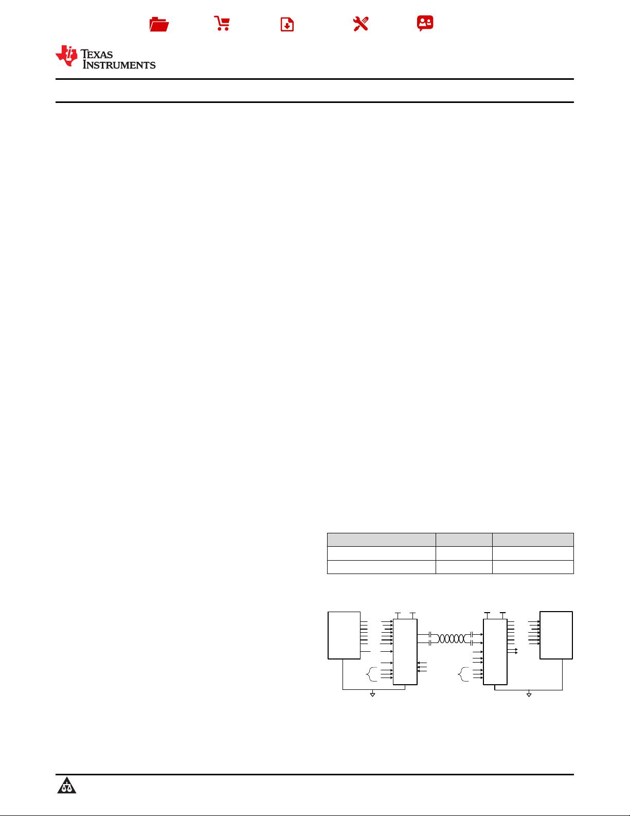
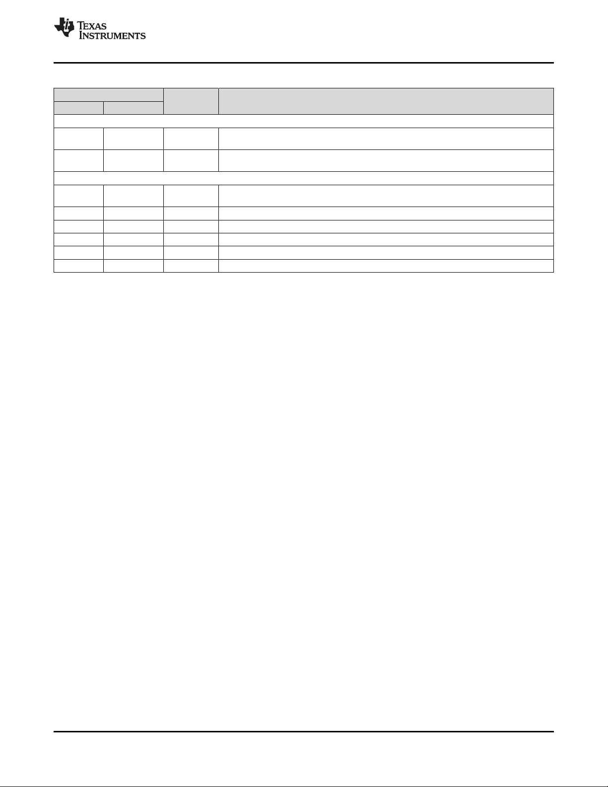
DI[7:0]
CI2
CI3
CLKIN
PDB
Serializer Deserializer
CI1
Graphic
Processor
Channel Link II
1 Pair / AC Coupled
DS92LV2411 DS92LV2412
100 ohm STP Cable
PASS
V
DDIO
PDB
SCL
SDA
RFB
VODSEL
DeEmph
BISTEN
BISTEN
LOCK
ID[x]
DAP DAP
CMF
0.1 PF 0.1 PF
SCL
SDA
ID[x]
STRAP pins
not shown
RIN+
RIN-
DOUT+
DOUT-
Optional Optional
(1.8V or 3.3V)(1.8V or 3.3V)
1.8V
1.8V
V
DDIO
V
DDn
V
DDn
ASIC/FPGA
OR
24-bit RGB
Display
ASIC/FPGA
OR
DI[15:8]
DI[23:16]
DO[7:0]
CO2
CO3
CLKOUT
CO1
DO[15:8]
DO[23:16]
Video
Imager
OR
Product
Folder
Sample &
Buy
Technical
Documents
Tools &
Software
Support &
Community
DS92LV2411
,
DS92LV2412
SNLS302E –MAY 2010–REVISED FEBRUARY 2015
DS92LV241x 5 to 50 MHz 24-Bit Channel Link II Serializer And Deserializer
1 Features 3 Description
The DS92LV2411 (Serializer) and DS92LV2412
1
• 24-Bit Data, 3–Bit Control, 5 to 50 MHz Clock
(Deserializer) chipset translates a parallel 24–bit
• Application Payloads up to 1.2 Gbps
LVCMOS data interface into a single high-speed CML
• AC Coupled Interconnects: STP up to 10 m or
serial interface with embedded clock information. This
Coax 20+ m
single serial stream eliminates skew issues between
clock and data, reduces connector size and
• 1.8 V or 3.3 V Compatible LVCMOS I/O Interface
interconnect cost for transferring a 24-bit, or less, bus
• Integrated Terminations on Ser and Des
over FR-4 printed circuit board backplanes,
• AT-SPEED BIST Mode and Reporting Pin
differential or coax cables.
• Configurable by Pins or I2C Compatible Serial
In addition to the 24-bit data bus interface, the
Control Bus
DS92LV2411/12 also features a 3-bit control bus for
• Power Down Mode Minimizes Power Dissipation
slow speed signals. This allows implementing video
and display applications with up to 24–bits per pixel
• >8 kV HBM ESD Rating
(RGB888).
• SERIALIZER — DS92LV2411
Programmable transmit de-emphasis, receive
– Supports Spread Spectrum Clocking (SSC) on
equalization, on-chip scrambling and DC balancing
Inputs
enables long distance transmission over lossy cables
– Data Scrambler for Reduced EMI
and backplanes. The DS92LV2412 automatically
locks to incoming data without an external reference
– DC-Balance Encoder for AC Coupling
clock or special sync patterns, providing easy “plug-
– Selectable Output V
OD
and Adjustable De-
and-go” or “hot plug” operation. EMI is minimized by
emphasis
the use of low voltage differential signaling, receiver
• DESERIALIZER — DS92LV2412
drive strength control, and spread spectrum clocking
capability.
– Random Data Lock; no Reference Clock
Required
The DS92LV2411/12 chipset is programmable though
– Adjustable Input Receiver Equalization
an I2C interface as well as through Pins. A built-in
AT-SPEED BIST feature validates link integrity and
– LOCK (Real Time Link Status) Reporting Pin
may be used for system diagnostics.
– Selectable Spread Spectrum Clock Generation
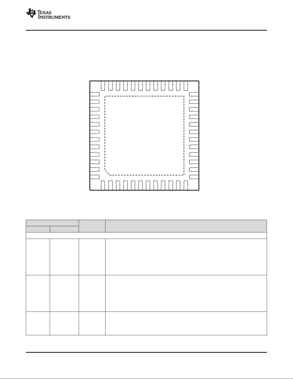
The DS92LV2411 is offered in a 48-Pin WQFN and
(SSCG) and Output Slew Rate Control (OS) to
the DS92LV2412 is offered in a 60-Pin WQFN
Reduce EMI
package. Both devices operate over the full industrial
temperature range of -40°C to +85°C.
2 Applications
• Embedded Video and Display
Device Information
• Medical Imaging
PART NUMBER PACKAGE BODY SIZE (NOM)
• Factory Automation
DS92LV2411 WQFN (48) 7.00 mm × 7.00 mm
DS92LV2412 WQFN (60) 9.00 mm × 9.00 mm
• Office Automation — Printer, Scanner
• Security and Video Surveillance
4 Typical Application Schematic
• General Purpose Data Communication
1
An IMPORTANT NOTICE at the end of this data sheet addresses availability, warranty, changes, use in safety-critical applications,
intellectual property matters and other important disclaimers. PRODUCTION DATA.
剩余57页未读,继续阅读
资源评论


