TI-DS92LV1224.pdf

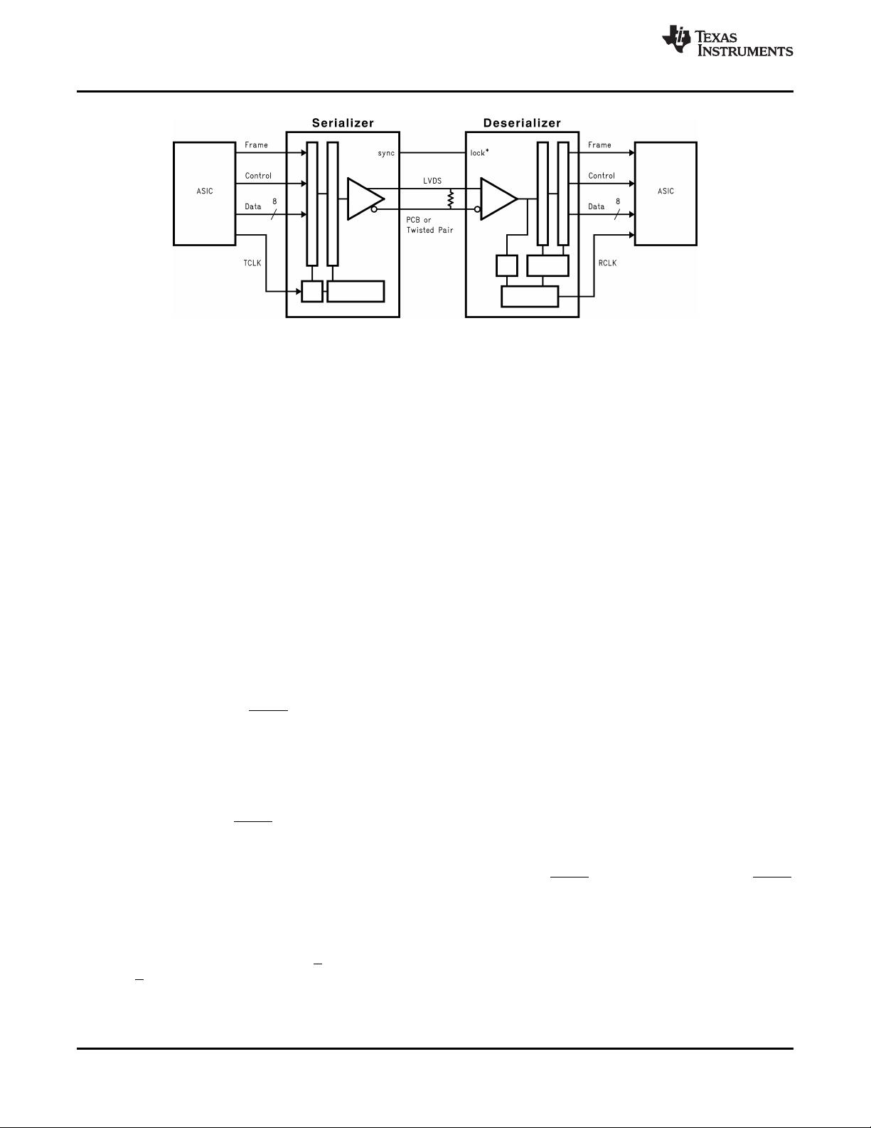
TI的DS92LV1224是一款专为高速单向串行数据传输设计的LVDS(低压差分信号)解串器。该器件适用于30到66MHz的频率范围,可实现300到660 Mb/s的数据吞吐率,特别适合在FR-4印刷电路板背板和平衡铜缆上简化PCB设计并降低成本。
**主要特性**
1. **30-66 MHz单1:10解串器**:DS92LV1224将接收到的与嵌入式时钟同步的10位宽Bus LVDS串行数据流转换回10位并行数据总线,并恢复并行时钟。这简化了数据路径,减少了PCB的尺寸和层数,降低了成本。
2. **时钟恢复功能**:从PLL锁定到随机数据模式,都能确保时钟的稳定恢复,提供出色的噪声免疫力和低EMI(电磁干扰)性能。
3. **每个数据转移周期确保转换**:确保每次数据传输时都有明确的转换,提高系统稳定性。
4. **低功耗**:在66 MHz工作时,典型功耗小于300 mW,降低了系统运行的能耗。
5. **单个差分对消除多通道 skew**:通过使用单个差分对,避免了多个通道之间的时钟与数据、数据与数据之间的偏移问题。
6. **流动式引脚布局**:设计有流动式引脚布局,便于PCB布局,节省空间。
7. **同步模式和锁定指示器**:提供同步模式和锁定状态指示,方便系统监控和调试。
8. **可编程边沿触发时钟**:用户可以根据需求设置时钟触发边缘,增强了系统的灵活性。
9. **电源关闭时高阻抗接收输入**:当电源关闭时,接收输入端进入高阻抗状态,防止未定义的信号输入。
10. **小型28引脚SSOP封装**:采用28引脚的小型表面贴装封装,节省板级空间。
**工作原理**
DS92LV1224的工作流程主要包括两个部分:串行至并行转换和时钟恢复。串行输入通过PLL(锁相环)进行同步和解码,然后通过10位并行输出latch将数据转换为并行格式。同时,时钟恢复单元从串行数据流中提取并恢复出原始的并行时钟。该器件的锁定指示器会显示PLL是否成功锁定到数据流,确保数据的准确传输。
在设计PCB时,利用DS92LV1224的流动式引脚布局可以简化布线,减少信号间的相互干扰。此外,由于DS92LV1224支持低功耗运行,因此对于电池供电或能源敏感的应用来说,是一个理想的解决方案。
TI的DS92LV1224 LVDS解串器通过简化高速数据传输的硬件设计,提供了高效、低功耗且可靠的并行数据恢复方案,是高性能通信、数据中心和工业应用的理想选择。在使用此设备时,应遵循TI提供的标准保修和使用指南,特别是在关键应用中,确保设备的正确选型和使用。
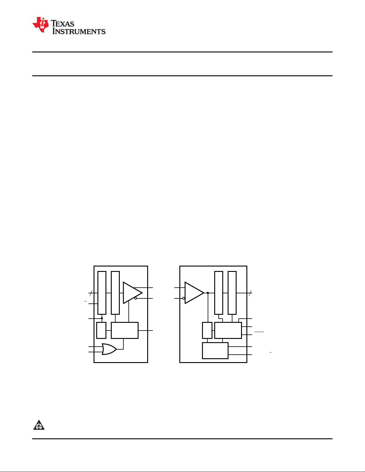
PARALLEL-TO-SERIAL
INPUT LATCH
TIMING and
CONTROL
PLL
10-BIT SERIALIZER
SYNC1
SYNC2
TCLK
(30 MHz to 66 MHz)
TCLK_R/F
D
IN
10
D
O+
D
O-
DEN
SERIAL-TO-PARALLEL
OUTPUT LATCH
R
I+
R
I-
LVDS
DS92LV1224
TIMING and
CONTROL
PLL
CLOCK
RECOVERY
10
R
OUT
REFCLK
REN
LOCK
RCLK
(30 MHz to 66 MHz)
RCLK_R/F
DS92LV1224
www.ti.com
SNLS189A –APRIL 2005–REVISED APRIL 2013
DS92LV1224 30-66 MHz 10 Bit Bus LVDS Deserializer
Check for Samples: DS92LV1224
1
FEATURES
DESCRIPTION
The DS92LV1224 is a 300 to 660 Mb/s deserializer
2
• 30–66 MHz Single 1:10 Deserializer with
for high-speed unidirectional serial data transmission
300–660 Mb/s Throughput
over FR-4 printed circuit board backplanes and
• Robust Bus LVDS Serial Data Transmission
balanced copper cables. It receives the Bus LVDS
with Embedded Clock for Exceptional Noise
serial data stream from a compatible 10–bit serializer,
Immunity and Low EMI
transforms it back into a 10-bit wide parallel data bus
and recovers parallel clock. This single serial data
• Clock Recovery from PLL Lock to Random
stream simplifies PCB design and reduces PCB cost
Data Patterns
by narrowing data paths that in turn reduce PCB size
• Ensured Transition Every Data Transfer Cycle
and number of layers. The single serial data stream
• Low Power Consumption < 300 mW (typ)
also reduces cable size, the number of connectors,
at 66 MHz
and eliminates clock-to-data and data-to-data skew.
• Single Differential Pair Eliminates Multi-
The DS92LV1224 works well with Bus LVDS 10–bit
Channel Skew
serializers within its specified frequency operating
range. It features low power consumption, and high
• Flow-Through Pinout for Easy PCB Layout
impedance outputs in power down mode.
• Synchronization Mode and LOCK Indicator
The DS92LV1224 was designed with the flow-through
• Programmable Edge Trigger on Clock
pinout and is available in a space saving 28–lead
• High Impedance on Receiver Inputs when
SSOP package.
Power is Off
• Small 28-Lead SSOP Package
Block Diagrams
1
Please be aware that an important notice concerning availability, standard warranty, and use in critical applications of
Texas Instruments semiconductor products and disclaimers thereto appears at the end of this data sheet.
2All trademarks are the property of their respective owners.
PRODUCTION DATA information is current as of publication date.
Copyright © 2005–2013, Texas Instruments Incorporated
Products conform to specifications per the terms of the Texas
Instruments standard warranty. Production processing does not
necessarily include testing of all parameters.

剩余22页未读,继续阅读
148 浏览量
2023-02-08 上传
2023-02-08 上传
171 浏览量
174 浏览量
139 浏览量
152 浏览量
2023-02-08 上传
192 浏览量
133 浏览量
2023-02-08 上传
资源评论

 2301_763960562023-02-15#完美解决问题 #运行顺畅 #内容详尽 #全网独家 #注释完整

不觉明了
- 粉丝: 7479
- 资源: 5764


最新资源
- 【锂电池剩余寿命预测】TCN时间卷积神经网络锂电池剩余寿命预测,马里兰大学锂电池数据集(Pytorch完整源码和数据)
- stm32 USB 复合设备使用msc cdc
- 武汉、西安等城市预处理后的路网数据,包括道路双线转单线、中心打断等等
- 【锂电池剩余寿命预测】Transformer锂电池剩余寿命预测,马里兰大学锂电池数据集(Pytorch完整源码和数据)
- 汽车电机壳体压装产线sw18可编辑全套技术资料100%好用.zip
- boot-win7.c2c84adb.mp4
- redis笔记自学笔记自学笔记
- 前端分析-2023071100789
- 工创赛k210视觉识别
- 前端分析-2023071100789
- Java 21 新特性详解:虚拟线程、字符串模板与模式匹配等亮点
- Photoshop-CS6-13.0.1-简化版
- 通过网盘分享的文件:中国国家级地面气象站基本气象要素日值数据集(V3.0)SURF-CLI-CHN-MUL-DAY-V3.0.zip
- AI游戏Flappy-Bird
- Java各版本新特性一览表,汇总Java 8~21的新特性,按功能分类速查
- 大模型与智能制造融合创新报告,涵盖智能制造背景、大模型技术赋能、工艺优化、智能研发、生产调度、供应链优化、数据安全等内容,助力制造业降本增效、智能化升级与高效决策,适用于行业报告撰写与企业战略规划
