TI-ADS131M03-Q1.pdf
需积分: 9 97 浏览量
2022-11-27
00:04:33
上传
评论 4
收藏 2.6MB PDF 举报

ADS131M03-Q1 汽车类、3 通道、64 kSPS、同步采样、24 位、Δ-Σ ADC
1 特性
• 符合面向汽车应用的 AEC-Q100 标准:
– 温度等级 1:–40°C 至 +125°C,T
A
• 提供功能安全型
– 有助于进行功能安全系统设计的文档
• 3 同步采样差分输入
• 可编程数据速率高达 64kSPS
• 可编程增益高达 128
• 噪声性能:
– 当增益为 1.4 kSPS 时,动态范围为 102dB
– 当增益为 64.4 kSPS 时,动态范围为 80dB
• 总谐波失真:-100dB
• 用于直接传感器连接的高阻抗输入:
– 当增益为 1、2 和 4 时,
输入阻抗为 330kΩ
– 当增益为 8、16、32、64 和 128 时,
输入阻抗 ≥ 1MΩ
• 可编程的通道间相位延迟校准:
– 分辨率 = 244 ns,f
CLKIN
= 8.192 MHz
• 快速启动:电压斜升 0.5 ms 内的第一个数据
• 集成的负电荷泵允许输入信号低于接地值
• 通道间串扰:-120 dB
• 低漂移内部电压基准
• 用于通信和寄存器映射的循环冗余校验器 (CRC)
• 模拟和数字电源:2.7V 至 3.6V
• 低功耗:3V AVDD 和 DVDD 下为 3.6mW
• 封装:20 引脚 TSSOP
2 应用
• 汽车电池管理系统 (BMS):
– 电流分流测量
– 使用外部电阻分压器实现电压测量
– 使用热敏电阻或模拟输出温度传感器实现温度测
量
• 电动汽车充电站:
– 直流电子计量
– 交流电子计量
• 能量存储系统 (ESS)
3 说明
ADS131M03-Q1 是一款 three 通道、同步采样、
24 位、Δ-Σ 模数转换器 (ADC),具有宽动态范围和低
功耗,因此非常适合用于汽车电池管理系统 (BMS)。
ADC 输入可以直接连接到分流电阻器以实现双向电池
电流测量,连接到电阻分压器网络以实现高电压测量,
或者连接到温度传感器(例如,热敏电阻或模拟输出温
度传感器)。
可以根据传感器输入独立配置各个 ADC 通道。低噪
声、可编程增益放大器 (PGA) 提供了从 1 到 128 的增
益,用以放大低电平信号。此外,该器件集成了通道间
相位校准、偏移和增益校准寄存器,有助于消除信号链
误差。
该器件集成了低漂移、1.2V 基准,减小了印刷电路板
(PCB) 面积。数据输入、数据输出和寄存器映射中可选
的循环冗余校验 (CRC) 确保了通信完整性。
完整的模拟前端 (AFE) 采用 20 引脚 TSSOP 封装,额
定汽车级温度范围为 –40°C 至 +125°C。
封装信息
(1)
器件型号 封装 封装尺寸(标称值)
ADS131M03-Q1 TSSOP (20) 6.50mm × 4.40mm
(1) 如需了解所有可用封装,请参阅数据表末尾的可订购产品附
录。
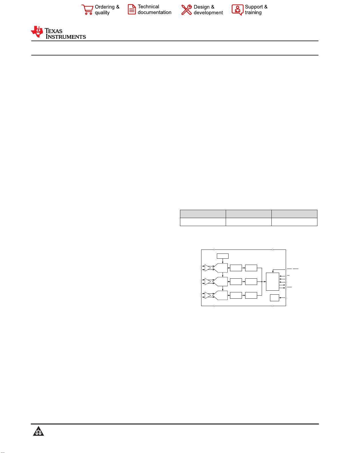
'6ADC
SCLK
DOUT
DIN
Control &
Serial Interface
CS
Gain & Offset
Calibration
AVDD
AGND
DVDD
DGND
DRDY
Clock
Generation
CLKIN
1.2-V
Reference
SYNC / RESET
Phase Shift &
Digital Filter
'6ADC
Gain & Offset
Calibration
Phase Shift &
Digital Filter
'6ADC
Gain & Offset
Calibration
Phase Shift &
Digital Filter
AIN0P
AIN0N
+
±
AIN1P
AIN1N
+
±
AIN2P
AIN2N
+
±
简化版方框图
ADS131M03-Q1
ZHCSPW1 – AUGUST 2022
本文档旨在为方便起见,提供有关 TI 产品中文版本的信息,以确认产品的概要。有关适用的官方英文版本的最新信息,请访问
www.ti.com,其内容始终优先。TI 不保证翻译的准确性和有效性。在实际设计之前,请务必参考最新版本的英文版本。
English Data Sheet: SBASAJ3

剩余85页未读,继续阅读


评论0
最新资源