没有合适的资源?快使用搜索试试~ 我知道了~
TI-ADS131M02-Q1.pdf
需积分: 9 0 下载量 83 浏览量
2022-11-27
00:04:51
上传
评论 4
收藏 2.31MB PDF 举报
温馨提示
试读
77页
TI-ADS131M02-Q1.pdf
资源推荐
资源详情
资源评论
ADS131M02-Q1 汽车类、2 通道、64 kSPS、同步采样、24 位、Δ-Σ ADC
1 Features
• AEC-Q100 qualified for automotive applications:
– Temperature grade 1: –40°C to +125°C, T
A
• Functional Safety-Capable
– Documentation available to aid functional safety
system design
• 2 simultaneously sampling differential inputs
• Programmable data rate up to 64 kSPS
• Programmable gain up to 128
• Noise performance:
– 102-dB dynamic range at gain = 1, 4 kSPS
– 80-dB dynamic range at gain = 64, 4 kSPS
• Total harmonic distortion: –100 dB
• High-impedance inputs for direct sensor
connection:
– 330-kΩ input impedance for gains of
1, 2, and 4
– ≥1-MΩ input impedance for gains of
8, 16, 32, 64, and 128
• Programmable channel-to-channel phase delay
calibration:
– Resolution = 244 ns, f
CLKIN
= 8.192 MHz
• Fast start-up: First data within 0.5 ms of supply
ramp
• Integrated negative charge pump allows input
signals below ground
• Crosstalk between channels: –120 dB
• Low-drift internal voltage reference
• Cyclic redundancy check (CRC) on
communications and register map
• Analog and digital supplies: 2.7 V to 3.6 V
• Low-power consumption: 2.3 mW at 3-V AVDD
and DVDD
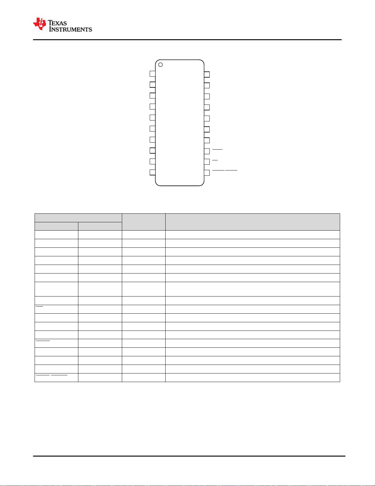
• Package: 20-pin TSSOP
2 Applications
• Automotive battery management systems (BMS):
– Current-shunt measurements
– Voltage measurements using external resistor
dividers
– Temperature measurements using thermistors
or analog output temperature sensors
• EV charging stations:
– DC e-metering
– AC e-metering
• Energy storage systems (ESS)
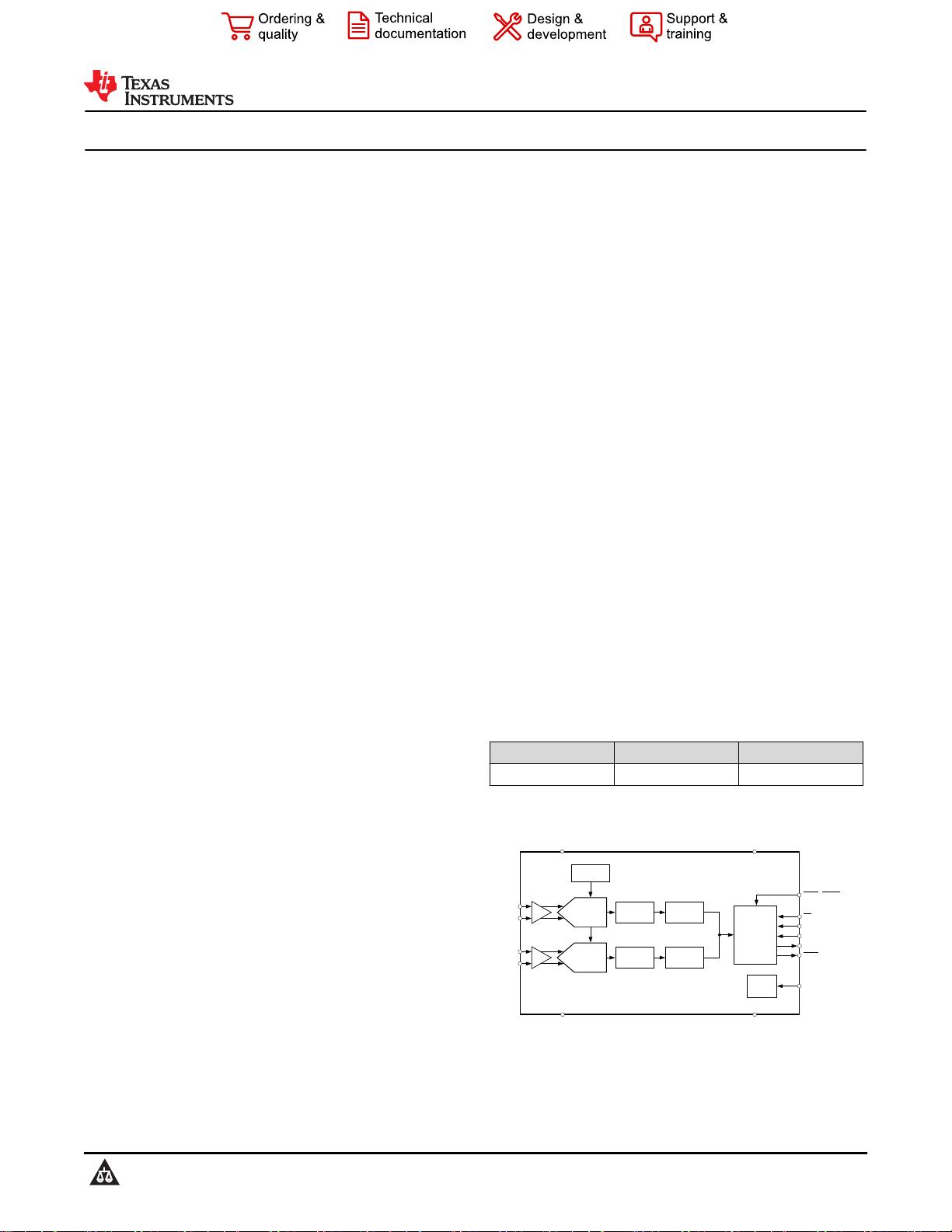
3 Description
The ADS131M02-Q1 is a two-channel, simultaneously
sampling, 24-bit, delta-sigma (
ΔΣ), analog-to-digital
converter (ADC) that offers wide dynamic range and
low power, making the device designed for automotive
battery management systems (BMS). The ADC inputs
can be directly interfaced to shunt resistors for
bidirectional battery-current measurements, to
resistor-divider networks for high-voltage
measurements, or to temperature sensors (such as
thermistors or analog output temperature sensors).
The individual ADC channels can be independently
configured depending on the sensor input. A low-
noise, programmable gain amplifier (PGA) provides
gains ranging from 1 to 128 to amplify low-level
signals. Additionally, this device integrates channel-to-
channel phase calibration and offset and gain
calibration registers to help remove signal-chain
errors.
A low-drift, 1.2-V reference is integrated into the
device, reducing printed circuit board (PCB) area.
Optional cyclic redundancy checks (CRCs) on the
data input, data output, and register map maintain
communication integrity.
The complete analog front-end (AFE) is offered in a
20-pin TSSOP package and is specified over the
automotive temperature range of –40°C to +125°C.
Package Information
(1)
PART NUMBER PACKAGE BODY SIZE (NOM)
ADS131M02-Q1 TSSOP (20) 6.50 mm × 4.40 mm
(1) For all available packages, see the orderable addendum at
the end of the data sheet.
'6ADC
SCLK
DOUT
DIN
Control &
Serial Interface
CS
Gain & Offset
Calibration
AVDD
AGND
DVDD
DGND
DRDY
Clock
Generation
CLKIN
1.2-V
Reference
SYNC / RESET
Phase Shift &
Digital Filter
'6ADC
Gain & Offset
Calibration
Phase Shift &
Digital Filter
AIN0P
AIN0N
+
±
AIN1P
AIN1N
+
±
Simplified Block Diagram
ADS131M02-Q1
ZHCSOL6 – AUGUST 2022
本文档旨在为方便起见,提供有关 TI 产品中文版本的信息,以确认产品的概要。有关适用的官方英文版本的最新信息,请访问
www.ti.com,其内容始终优先。TI 不保证翻译的准确性和有效性。在实际设计之前,请务必参考最新版本的英文版本。
English Data Sheet: SBASAE7
Table of Contents
1 Features............................................................................1
2 Applications..................................................................... 1
3 Description.......................................................................1
4 Revision History.............................................................. 2
5 Pin Configuration and Functions...................................3
6 Specifications.................................................................. 4
6.1 Absolute Maximum Ratings........................................ 4
6.2 ESD Ratings............................................................... 4
6.3 Recommended Operating Conditions.........................5
6.4 Thermal Information....................................................5
6.5 Electrical Characteristics.............................................6
6.6 Timing Requirements.................................................. 8
6.7 Switching Characteristics............................................8
6.8 Timing Diagrams....................................................... 10
6.9 Typical Characteristics.............................................. 11
7 Parameter Measurement Information.......................... 16
7.1 Noise Measurements................................................ 16
8 Detailed Description......................................................18
8.1 Overview................................................................... 18
8.2 Functional Block Diagram......................................... 18
8.3 Feature Description...................................................18
8.4 Device Functional Modes..........................................30
8.5 Programming............................................................ 36
8.6 ADS131M02-Q1 Registers....................................... 46
9 Application and Implementation.................................. 67
9.1 Application Information............................................. 67
9.2 Typical Application.................................................... 71
9.3 Power Supply Recommendations.............................74
9.4 Layout....................................................................... 74
10 Device and Documentation Support..........................76
10.1 Documentation Support.......................................... 76
10.2 接收文档更新通知................................................... 76
10.3 支持资源..................................................................76
10.4 Trademarks............................................................. 76
10.5 Electrostatic Discharge Caution..............................76
10.6 术语表..................................................................... 76
11 Mechanical, Packaging, and Orderable
Information.................................................................... 76
4 Revision History
注:以前版本的页码可能与当前版本的页码不同
DATE REVISION NOTES
August 2022 * Initial Release
ADS131M02-Q1
ZHCSOL6 – AUGUST 2022
www.ti.com.cn
2 Submit Document Feedback
Copyright © 2022 Texas Instruments Incorporated
Product Folder Links: ADS131M02-Q1
5 Pin Configuration and Functions
10
4
3
2
1
14
15
16
17
NC
AIN0P
CAP
CLKIN
AGND
DIN
AIN1N
AIN0N
NC
13
DOUT
9
NC
AIN1P
5
8
7
6
18
19
20
AVDD
NC
DVDD
DRDY
SCLK
CS
DGND
11
12
SYNC / RESET
图 5-1. PW Package, 20-Pin TSSOP (Top View)
表 5-1. Pin Functions
PIN
I/O DESCRIPTION
(1)
NAME NO.
AGND 2 Supply Analog ground
AIN0N 4 Analog input Negative analog input 0
AIN0P 3 Analog input Positive analog input 0
AIN1N 5 Analog input Negative analog input 1
AIN1P 6 Analog input Positive analog input 1
AVDD 1 Supply Analog supply. Connect a 1-µF capacitor to AGND.
CAP 18 Analog output
Digital low-dropout (LDO) regulator output.
Connect a 220-nF capacitor to DGND.
CLKIN 17 Digital input Main clock input
CS 12 Digital input Chip select; active low
DGND 19 Supply Digital ground
DIN 16 Digital input Serial data input
DOUT 15 Digital output Serial data output
DRDY 13 Digital output Data ready; active low
DVDD 20 Supply Digital I/O supply. Connect a 1-µF capacitor to DGND.
NC 7, 8, 9, 10
—
Leave unconnected or connect to AGND
SCLK 14 Digital input Serial data clock
SYNC/RESET 11 Digital input Conversion synchronization or system reset; active low
(1) See the Unused Inputs and Outputs section for details on how to connect unused pins.
www.ti.com.cn
ADS131M02-Q1
ZHCSOL6 – AUGUST 2022
Copyright © 2022 Texas Instruments Incorporated
Submit Document Feedback
3
Product Folder Links: ADS131M02-Q1
6 Specifications
6.1 Absolute Maximum Ratings
see
(1)
MIN MAX UNIT
Power-supply voltage
AVDD to AGND
–0.3
3.9
V
AGND to DGND
–0.3
0.3
DVDD to DGND
–0.3
3.9
DVDD to DGND, CAP tied to DVDD
–0.3
2.2
CAP to DGND
–0.3
2.2
Analog input voltage AINxP, AINxN
AGND – 1.6
AVDD + 0.3
Digital input voltage CS, CLKIN, DIN, SCLK, SYNC/RESET
DGND – 0.3
DVDD + 0.3
Input current Continuous, all pins except power-supply pins
–10
10 mA
Temperature
Junction, T
J
150
°C
Storage, T
stg
–60
150
(1) Operation outside the Absolute Maximum Ratings may cause permanent device damage. Absolute Maximum Ratings do not imply
functional operation of the device at these or any other conditions beyond those listed under Recommended Operating Conditions. If
used outside the Recommended Operating Conditions but within the Absolute Maximum Ratings, the device may not be fully
functional, and this may affect device reliability, functionality, performance, and shorten the device lifetime.
6.2 ESD Ratings
VALUE UNIT
V
(ESD)
Electrostatic discharge
Human-body model (HBM),
per AEC Q100-002
(1)
HBM ESD classification level 2
±2000
V
Charged-device model (CDM),
per AEC Q100-011
CDM ESD classification level C4B
Corner pins ±750
All other non-corner pins ±500
(1) AEC Q100-002 indicates that HBM stressing shall be in accordance with the ANSI/ESDA/JEDEC JS-001 specification.
ADS131M02-Q1
ZHCSOL6 – AUGUST 2022
www.ti.com.cn
4 Submit Document Feedback
Copyright © 2022 Texas Instruments Incorporated
Product Folder Links: ADS131M02-Q1
6.3 Recommended Operating Conditions
over operating ambient temperature range (unless otherwise noted)
MIN NOM MAX UNIT
POWER SUPPLY
Analog power supply
AVDD to AGND, normal operating modes 2.7 3.0 3.6
V
AVDD to AGND, standby and current-detect
modes
2.4 3.0 3.6
AGND to DGND
–0.3
0 0.3
Digital power supply
DVDD to DGND 2.7 3.0 3.6
V
DVDD to DGND, DVDD shorted to CAP
(digital LDO bypassed)
1.65 1.8 2
ANALOG INPUTS
(1)
V
AINxP
,
V
AINxN
Absolute input voltage
Gain = 1, 2, or 4
AGND –
1.3
AVDD
V
Gain = 8, 16, 32, 64 or 128
AGND –
1.3
AVDD – 1.8
V
IN
Differential input voltage V
IN
= V
AINxP
- V
AINxN
–V
REF
/
Gain
V
REF
/ Gain V
EXTERNAL CLOCK SOURCE
f
CLKIN
External clock frequency
High-resolution mode 0.3 8.192 8.4
MHzLow-power mode 0.3 4.096 4.15
Very-low-power mode 0.3 2.048 2.08
Duty cycle 40% 50% 60%
DIGITAL INPUTS
Input voltage DGND DVDD V
TEMPERATURE RANGE
T
A
Operating ambient temperature
–40
125 °C
(1) The subscript "x" signifies the channel. For example, the positive analog input to channel 0 is named AIN0P. See the Pin Configuration
and Functions section for the pin names.
6.4 Thermal Information
THERMAL METRIC
(1)
ADS131M02-Q1
UNITPW (TSSOP)
20 PINS
R
θJA
Junction-to-ambient thermal resistance 94.9 °C/W
R
θ
JC(top)
Junction-to-case (top) thermal resistance 34.9 °C/W
R
θJB
Junction-to-board thermal resistance 46.4 °C/W
Ψ
JT
Junction-to-top characterization parameter 2.7 °C/W
Ψ
JB
Junction-to-board characterization parameter 46.0 °C/W
R
θ
JC(bot)
Junction-to-case (bottom) thermal resistance N/A °C/W
(1) For more information about traditional and new thermal metrics, see the Semiconductor and IC Package Thermal Metrics application
report.
www.ti.com.cn
ADS131M02-Q1
ZHCSOL6 – AUGUST 2022
Copyright © 2022 Texas Instruments Incorporated
Submit Document Feedback
5
Product Folder Links: ADS131M02-Q1
剩余76页未读,继续阅读
资源评论
不觉明了
- 粉丝: 3101
- 资源: 5337
上传资源 快速赚钱
- 我的内容管理 展开
- 我的资源 快来上传第一个资源
- 我的收益 登录查看自己的收益
- 我的积分 登录查看自己的积分
- 我的C币 登录后查看C币余额
- 我的收藏
- 我的下载
- 下载帮助
安全验证
文档复制为VIP权益,开通VIP直接复制
信息提交成功