TI-ADS130B04-Q1.pdf
需积分: 9 138 浏览量
2022-11-27
16:53:43
上传
评论 4
收藏 1.72MB PDF 举报

ADS130B04-Q1 Automotive, 4-Channel, 32-kSPS, Simultaneous-Sampling,
16-Bit, Delta-Sigma ADC
1 Features
• AEC-Q100 qualified for automotive applications:
– Temperature grade 1: –40°C to +125°C, T
A
• Functional Safety-Capable
– Documentation available to aid functional safety
system design
• 4 simultaneous-sampling, differential input ADCs
• Programmable data rate: Up to 32 kSPS
• Programmable gain: Up to 128
• Global-chop mode to remove offset drift over
temperature and time
• High-impedance analog inputs for direct sensor
connection
• Integrated negative charge pump allows input
signal measurements below ground
• Crosstalk between channels: –120 dB
• Low-drift internal reference: 1.2 V
• Precision internal oscillator
• CRC on communications and register map
• Analog and digital supplies: 2.7 V to 3.6 V
• Low power consumption: 5 mW at 3.3-V AVDD
and DVDD
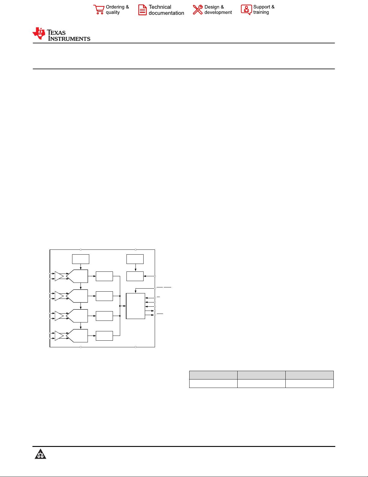
ADC
SCLK
DOUT
DIN
CS
AVDD
AGND
DVDD
DGND
DRDY
Oscillator
CLKIN
1.2-V
Reference
SYNC/RESET
Digital Filter
ADC
Digital Filter
ADC
Digital Filter
ADC
Digital Filter
AIN0P
AIN0N
+
–
AIN1P
AIN1N
+
–
AIN2P
AIN2N
+
–
AIN3P
AIN3N
+
–
Control &
Serial Interface
Clock
Selection
Simplified Block Diagram
2 Applications
• Automotive battery management systems (BMS):
– Current-shunt measurements
– Voltage measurements using external resistor
dividers
– Temperature measurements using thermistors
or analog output temperature sensors
• EV charging stations:
– DC e-metering
• Energy storage systems (ESS)
3 Description
The ADS130B04-Q1 is a four-channel, simultaneous-
sampling, 16-bit, delta-sigma (ΔΣ) analog-to-digital
converter (ADC) that offers wide dynamic range, low
power, and buffered analog inputs, making the device
an excellent fit for automotive battery management
systems (BMS). The ADC inputs can be directly
interfaced to shunt resistors for bidirectional battery-
current measurements, to resistor-divider networks
for high-voltage measurements, or to temperature
sensors (such as thermistors or analog output
temperature sensors).
The individual ADC channels can be independently
configured depending on the sensor input. A low-
noise, programmable gain amplifier (PGA) provides
gains ranging from 1 to 128 to amplify low-level
signals. The device features a global-chop mode to
remove offset drift over temperature and time.
A low-drift, 1.2-V reference and precision oscillator
are integrated into the device reducing printed circuit
board (PCB) area. Optional cyclic redundancy checks
(CRCs) on the data input, data output, and register
map maintain communication integrity.
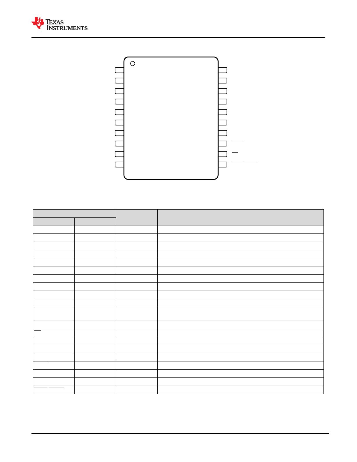
The complete analog front-end (AFE) is offered in
a 20-pin TSSOP package and is specified over the
automotive temperature range of –40°C to +125°C.
Device Information
(1)
PART NUMBER PACKAGE BODY SIZE (NOM)
ADS130B04-Q1 TSSOP (20) 6.50 mm × 4.40 mm
(1) For all available packages, see the orderable addendum at
the end of the data sheet.
ADS130B04-Q1
SBASAD2 – NOVEMBER 2021
An IMPORTANT NOTICE at the end of this data sheet addresses availability, warranty, changes, use in safety-critical applications,
intellectual property matters and other important disclaimers. PRODUCTION DATA.


剩余59页未读,继续阅读
资源评论


