TI-DS32EV400.pdf
需积分: 0 196 浏览量
2023-02-07
23:00:42
上传
评论 4
收藏 1.5MB PDF 举报


DS32EV400
www.ti.com
SNLS280F –AUGUST 2007–REVISED APRIL 2013
DisplayPort™ Quad Equalizer
Check for Samples: DS32EV400
1
FEATURES
DESCRIPTION
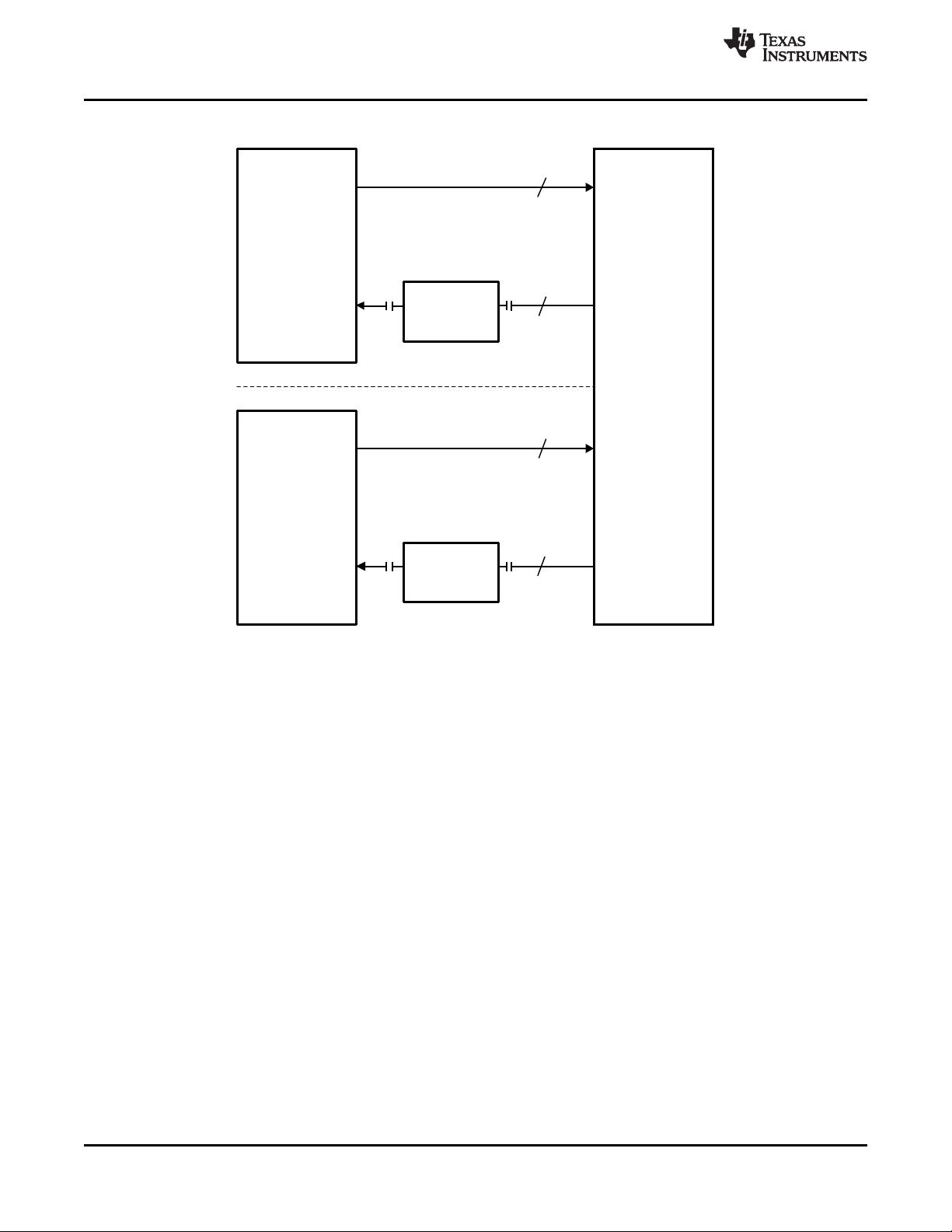
The DS32EV400 programmable quad equalizer
23
• Equalizes up to 14 dB Loss at 3.2 Gbps
provides compensation for transmission medium
• 8 Levels of Programmable Equalization
losses and reduces the medium-induced deterministic
• Settable Through Control Pins or SMBus
jitter for four NRZ data channels. The DS32EV400 is
Interface
optimized for operation up to 3.2 Gbps for both
cables and FR4 traces. Each equalizer channel has
• Operates up to 3.2 Gbps With 40” FR4 Traces
eight levels of input equalization that can be
• 0.12 UI Residual Deterministic Jitter at 3.2
programmed by three control pins, or individually
Gbps With 40” FR4 Traces
through a Serial Management Bus (SMBus) interface.
• Single 2.5V or 3.3V Power Supply
The device equalizes up to 14 dB of loss at 3.2 Gbps.
• Signal Detect for Individual Channels
The equalizer supports both AC and DC-coupled data
paths for long run length data patterns such as
• Standby Mode for Individual Channels
PRBS-31, and balanced codes such as 8b/10b. The
• Supports AC or DC-Coupling With Wide Input
device uses differential current-mode logic (CML)
Common-Mode
inputs and outputs.
• Low Power Consumption: 375 mW Typ at 2.5V
Each channel has an independent signal detect
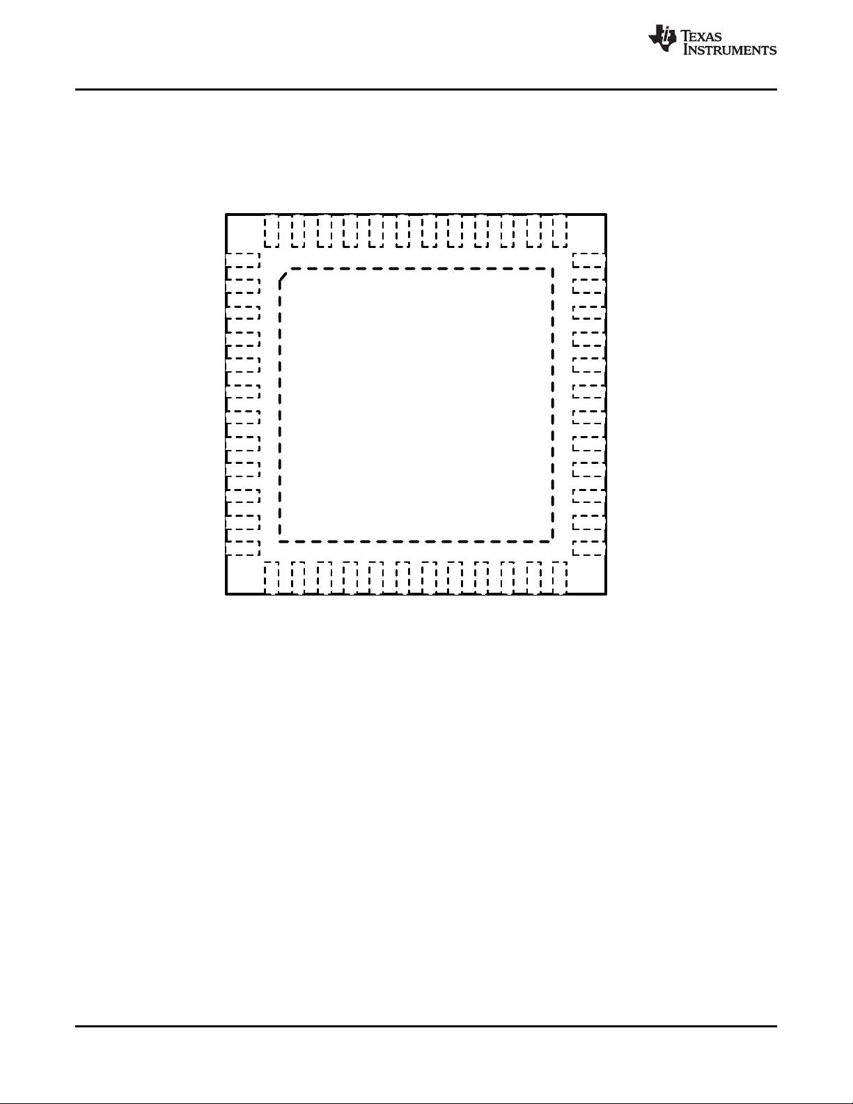
• Small 7 mm x 7 mm 48-pin WQFN Package
output and independent enable input. The SD output
• 9 kV HBM ESD Rating
maybe tied to the EN to automatically control the
power up and down of the channel.
• -40 to 85°C Operating Temperature Range
The DS32EV400 can be used in a variety of
APPLICATIONS
applications that include DisplayPort, XAUI,
InfiniBand and other high-speed data transmission
• DisplayPort
applications.
• XAUI
The DS32EV400 is available in a 7 mm x 7 mm 48-
• InfiniBand
pin leadless WQFN package. Power is supplied from
• Other 8b10b Applications
either a 2.5V or 3.3V supply.
1
Please be aware that an important notice concerning availability, standard warranty, and use in critical applications of
Texas Instruments semiconductor products and disclaimers thereto appears at the end of this data sheet.
2DisplayPort is a trademark of Video Electronics Standards Association (VESA)..
3All other trademarks are the property of their respective owners.
PRODUCTION DATA information is current as of publication date.
Copyright © 2007–2013, Texas Instruments Incorporated
Products conform to specifications per the terms of the Texas
Instruments standard warranty. Production processing does not
necessarily include testing of all parameters.
剩余22页未读,继续阅读
资源评论


