没有合适的资源?快使用搜索试试~ 我知道了~
TI-DS90CP22.pdf
需积分: 5 0 下载量 133 浏览量
2022-12-03
09:46:56
上传
评论 4
收藏 1.14MB PDF 举报
温馨提示
试读
19页
TI-DS90CP22.pdf
资源推荐
资源详情
资源评论
DS90CP22
www.ti.com
SNLS053E –MARCH 2000–REVISED APRIL 2013
DS90CP22 800 Mbps 2x2 LVDS Crosspoint Switch
Check for Samples: DS90CP22
1
FEATURES
DESCRIPTION
DS90CP22 is a 2x2 crosspoint switch utilizing LVDS
2
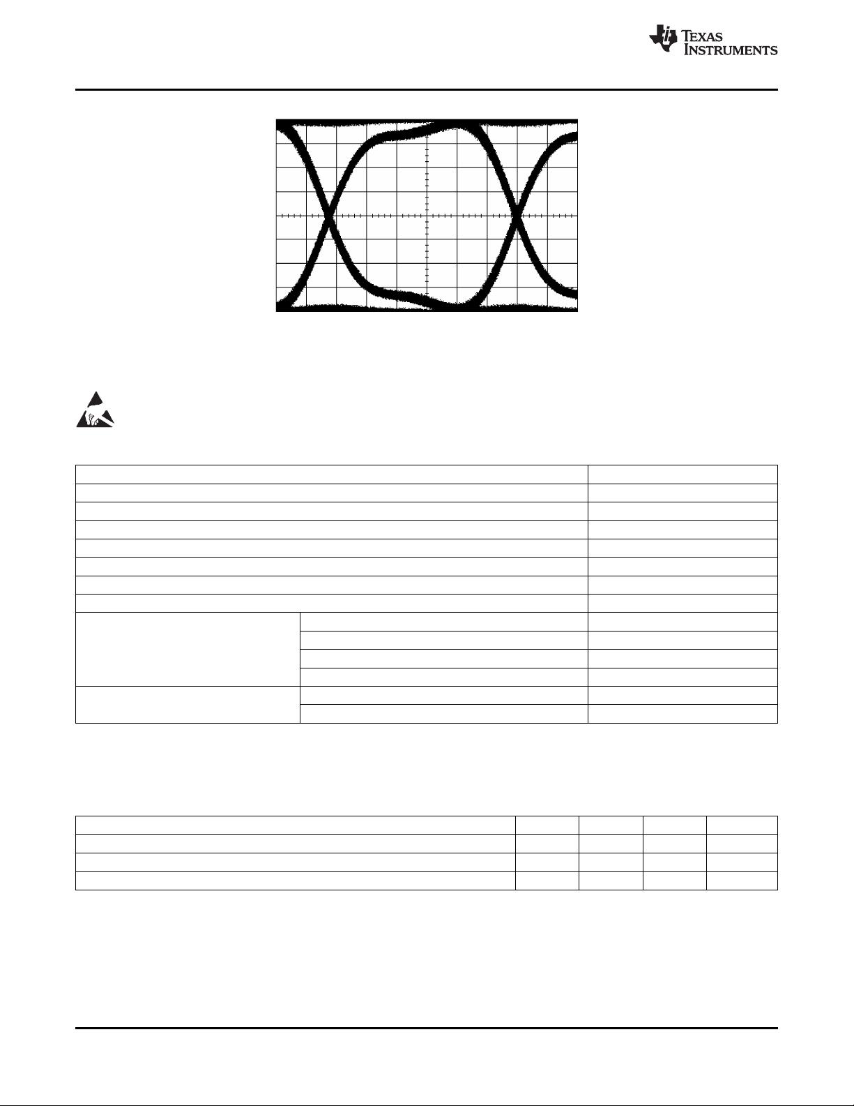
• DC - 800 Mbps Low Jitter, Low Skew Operation
(Low Voltage Differential Signaling) technology for
• 65 ps (typ) of Pk-Pk Jitter with PRBS = 2
23
−1
low power, high speed operation. Data paths are fully
Data Pattern at 800 Mbps
differential from input to output for low noise
• Single +3.3 V Supply
generation and low pulse width distortion. The non-
blocking design allows connection of any input to any
• Less than 330 mW (typ) Total Power
output or outputs. LVDS I/O enable high speed data
Dissipation
transmission for point-to-point interconnects. This
• Non-Blocking "'Switch Architecture"'
device can be used as a high speed differential
• Balanced Output Impedance
crosspoint, 2:1 mux, 1:2 demux, repeater or 1:2
signal splitter. The mux and demux functions are
• Output Channel-to-Channel Skew is 35 ps (typ)
useful for switching between primary and backup
• Configurable as 2:1 mux, 1:2 demux, Repeater
circuits in fault tolerant systems. The 1:2 signal
or 1:2 Signal Splitter
splitter and 2:1 mux functions are useful for
• LVDS Receiver Inputs Accept LVPECL Signals distribution of serial bus across several rack-mounted
backplanes.
• Fast Switch Time of 1.2ns (typ)
The DS90CP22 accepts LVDS signal levels, LVPECL
• Fast Propagation Delay of 1.3ns (typ)
levels directly or PECL with attenuation networks.
• Receiver Input Threshold < ±100 mV
The individual LVDS outputs can be put into TRI-
• Available in 16 Lead TSSOP and SOIC
STATE by use of the enable pins.
Packages
• Conforms to ANSI/TIA/EIA-644-1995 LVDS For more details, please refer to the Application
Information section of this datasheet.
Standard
• Operating Temperature: −40°C to +85°C
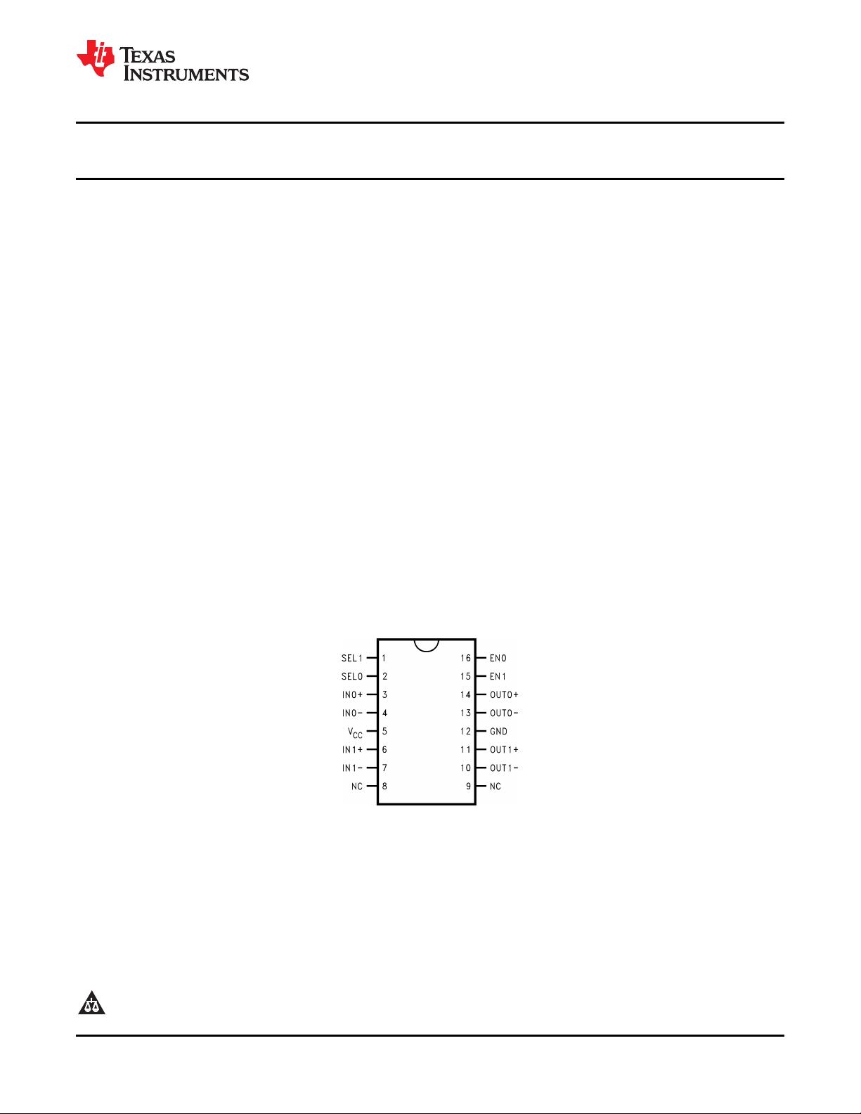
Connection Diagram
Figure 1. SOIC-16 Package
or
TSSOP-16 Package
1
Please be aware that an important notice concerning availability, standard warranty, and use in critical applications of
Texas Instruments semiconductor products and disclaimers thereto appears at the end of this data sheet.
2All trademarks are the property of their respective owners.
PRODUCTION DATA information is current as of publication date.
Copyright © 2000–2013, Texas Instruments Incorporated
Products conform to specifications per the terms of the Texas
Instruments standard warranty. Production processing does not
necessarily include testing of all parameters.
DS90CP22
SNLS053E –MARCH 2000–REVISED APRIL 2013
www.ti.com
Figure 2. Diff. Output Eye-Pattern in 1:2 split mode @ 800 Mbps
Conditions: 3.3 V, PRBS = 2
23
−1 data pattern,
V
ID
= 300mV, V
CM
= +1.2 V, 200 ps/div, 100 mV/div
These devices have limited built-in ESD protection. The leads should be shorted together or the device placed in conductive foam
during storage or handling to prevent electrostatic damage to the MOS gates.
Absolute Maximum Ratings
(1)(2)
Supply Voltage (V
CC
) −0.3V to +4V
CMOS/TTL Input Voltage (EN0, EN1, SEL0, SEL1) −0.3V to (V
CC
+ 0.3V)
LVDS Receiver Input Voltage (IN+, IN−) −0.3V to +4V
LVDS Driver Output Voltage (OUT+, OUT−) −0.3V to +4V
LVDS Output Short Circuit Current Continuous
Junction Temperature +150°C
Storage Temperature Range −65°C to +150°C
Lead Temperature (Soldering, 4 sec.) +260°C
Maximum Package Power Dissipation at 16L SOIC 1.435 W
25°C
16L SOIC Package Derating 11.48 mW/°C above +25°C
16L TSSOP 0.866 W
16L TSSOP Package Derating 9.6 mW/°C above +25°C
ESD Rating (HBM, 1.5kΩ, 100pF) > 5 kV
(EIAJ, 0Ω, 200pF) > 250 V
(1) If Military/Aerospace specified devices are required, please contact the Texas Instruments Sales Office/Distributors for availability and
specifications.
(2) “Absolute Maximum Ratings” are these beyond which the safety of the device cannot be verified. They are not meant to imply that the
device should be operated at these limits. “Electrical Characteristics” provides conditions for actual device operation.
Recommended Operating Conditions
Min Typ Max Units
Supply Voltage (V
CC
) 3.0 3.3 3.6 V
Receiver Input Voltage 0 V
CC
V
Operating Free Air Temperature -40 +25 +85 °C
2 Submit Documentation Feedback Copyright © 2000–2013, Texas Instruments Incorporated
Product Folder Links: DS90CP22
DS90CP22
www.ti.com
SNLS053E –MARCH 2000–REVISED APRIL 2013
Electrical Characteristics
(1)
Over recommended operating supply and temperature ranges unless otherwise specified
Symbol Parameter Conditions Min Typ Max Units
CMOS/TTL DC SPECIFICATIONS (EN0,EN1,SEL0,SEL1)
V
IH
High Level Input Voltage 2.0 V
CC
V
V
IL
Low Level Input Voltage GND 0.8 V
I
IH
High Level Input Current V
IN
= 3.6V or 2.0V; V
CC
= 3.6V +7 +20 μA
I
IL
Low Level Input Current V
IN
= 0V or 0.8V; V
CC
= 3.6V ±1 ±10 μA
V
CL
Input Clamp Voltage I
CL
= −18 mA −0.8 −1.5 V
LVDS OUTPUT DC SPECIFICATIONS (OUT0,OUT1)
V
OD
Differential Output Voltage R
L
= 75Ω 270 365 475 mV
R
L
= 75Ω, V
CC
= 3.3V, T
A
= 25°C 285 365 440 mV
ΔV
OD
Change in V
OD
between Complimentary Output States 35 mV
V
OS
Offset Voltage
(2)
1.0 1.2 1.45 V
ΔV
OS
Change in V
OS
between Complimentary Output States 35 mV
I
OZ
Output TRI-STATE Current TRI-STATE Output, ±1 ±10 μA
V
OUT
= V
CC
or GND
I
OFF
Power-Off Leakage Current V
CC
= 0V; V
OUT
= 3.6V or GND ±1 ±10 μA
I
OS
Output Short Circuit Current V
OUT+
OR V
OUT−
= 0V −15 −25 mA
I
OSB
Both Outputs Short Circuit Current V
OUT+
AND V
OUT−
= 0V −30 −50 mA
LVDS RECEIVER DC SPECIFICATIONS (IN0,IN1)
V
TH
Differential Input High Threshold V
CM
= +0.05V or +1.2V or +3.25V, 0 +100 mV
V
TL
Differential Input Low Threshold Vcc = 3.3V −100 0 mV
V
CMR
Common Mode Voltage Range V
ID
= 100mV, Vcc = 3.3V 0.05 3.25 V
I
IN
V
IN
= +3.0V, V
CC
= 3.6V or 0V ±1 ±10 μA
Input Current
V
IN
= 0V, V
CC
= 3.6V or 0V ±1 ±10 μA
SUPPLY CURRENT
I
CCD
Total Supply Current R
L
= 75Ω, C
L
= 5 pF, EN0 = EN1 = High 98 125 mA
I
CCZ
TRI-STATE Supply Current EN0 = EN1 = Low 43 55 mA
(1) All typical are given for V
CC
= +3.3V and T
A
= +25°C, unless otherwise stated.
(2) V
OS
is defined and measured on the ATE as (V
OH
+ V
OL
) / 2.
AC Electrical Characteristics
Over recommended operating supply and temperature ranges unless otherwise specified
(1)
Symbol Parameter Conditions Min Typ Max Units
T
SET
Input to SEL Setup Time
(2)
, (Figure 3 and Figure 4) 0.7 0.5 ns
T
HOLD
Input to SEL Setup Time
(2)
, (Figure 3 and Figure 4) 1.0 0.5 ns
T
SWITCH
SEL to Switched Output, (Figure 3 and Figure 4) 0.9 1.2 1.7 ns
T
PHZ
Disable Time (Active to TRI-STATE) High to Z, Figure 5 2.1 4.0 ns
T
PLZ
Disable Time (Active to TRI-STATE) Low to Z, Figure 5 3.0 4.5 ns
T
PZH
Enable Time (TRI-STATE to Active) Z to High, Figure 5 25.5 55.0 ns
T
PZL
Enable Time (TRI-STATE to Active) Z to Low, Figure 5 25.5 55.0 ns
T
LHT
Output Low-to-High Transition Time, 20% to 80%, Figure 7 290 400 580 ps
T
HLT
Output High-to-Low Transition Time, 80% to 20%, Figure 7 290 400 580 ps
(1) The parameters are specified by design. The limits are based on statistical analysis of the device performance over PVT (process,
voltage and temperature) range.
(2) T
SET
and T
HOLD
time specify that data must be in a stable state before and after the SEL transition.
Copyright © 2000–2013, Texas Instruments Incorporated Submit Documentation Feedback 3
Product Folder Links: DS90CP22
DS90CP22
SNLS053E –MARCH 2000–REVISED APRIL 2013
www.ti.com
AC Electrical Characteristics (continued)
Over recommended operating supply and temperature ranges unless otherwise specified
(1)
Symbol Parameter Conditions Min Typ Max Units
T
JIT
V
ID
= 300mV; 50% Duty Cycle; V
CM
=
40 90 ps
1.2V at 800Mbps
LVDS Data Path Peak to Peak Jitter
(3)
V
ID
= 300mV; PRBS=2
23
-1 data
65 120 ps
pattern; V
CM
= 1.2V at 800Mbps
T
PLHD
Propagation Low to High Delay, Figure 8 0.9 1.3 1.6 ns
Propagation Low to High Delay, Figure 8 V
CC
= 3.3V, T
A
= 25°C 1.0 1.3 1.5 ns
T
PHLD
Propagation High to Low Delay, Figure 8 0.9 1.3 1.6 ns
Propagation High to Low Delay, Figure 8 V
CC
= 3.3V, T
A
= 25°C 1.0 1.3 1.5 ns
T
SKEW
Pulse Skew |T
PLHD
- T
PHLD
| 0 225 ps
T
CCS
Output Channel-to-Channel Skew, Figure 9 35 80 ps
(3) The parameters are specified by design. The limits are based on statistical analysis of the device performance over PVT range with the
following equipment test setup: HP70004A (display mainframe) with HP70841B (pattern generator), 5 feet of RG-142 cable with DUT
test board and HP83480A (digital scope mainframe) with HP83483A (20GHz scope module).
AC Timing Diagrams
Figure 3. Input-to-Select rising edge setup and hold times and mux switch time
Figure 4. Input-to-Select falling edge setup and hold times and mux switch time
4 Submit Documentation Feedback Copyright © 2000–2013, Texas Instruments Incorporated
Product Folder Links: DS90CP22
剩余18页未读,继续阅读
资源评论
不觉明了
- 粉丝: 3175
- 资源: 5443
上传资源 快速赚钱
- 我的内容管理 展开
- 我的资源 快来上传第一个资源
- 我的收益 登录查看自己的收益
- 我的积分 登录查看自己的积分
- 我的C币 登录后查看C币余额
- 我的收藏
- 我的下载
- 下载帮助
安全验证
文档复制为VIP权益,开通VIP直接复制
信息提交成功