TI-DS64EV100.pdf
需积分: 5 97 浏览量
2022-12-04
00:17:44
上传
评论 3
收藏 1.59MB PDF 举报

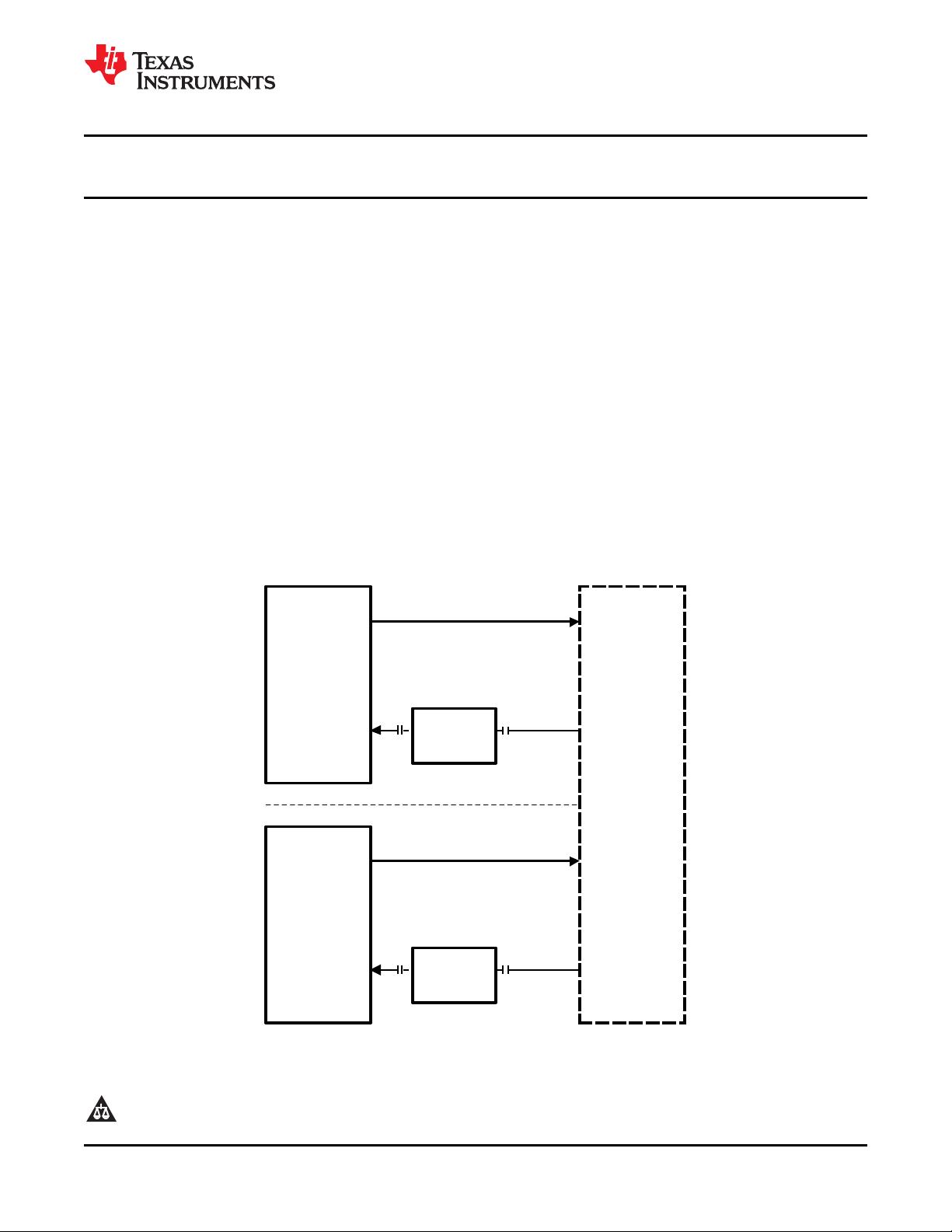
ASIC/FPGA
High Speed
I/O
Backplane/Cable
Sub-system
Switch Fabric Card
Line Card
OUT IN
DS64EV100
OUT IN
Tx
Tx
Rx
Rx
ASIC/FPGA
High Speed
I/O
DS64EV100
DS64EV100
www.ti.com
SNLS232E –OCTOBER 2006–REVISED FEBRUARY 2013
DS64EV100 Programmable Single Equalizer
Check for Samples: DS64EV100
1
FEATURES
DESCRIPTION
The DS64EV100 programmable equalizer provides
2
• Equalizes up to 24 dB loss at 10 Gbps
compensation for transmission medium losses and
• Equalizes up to 22 dB loss at 6.4 Gbps
reduces the medium-induced deterministic jitter for
• 8 levels of programmable equalization
NRZ data channel. The DS64EV100 is optimized for
operation up to 10 Gbps for both cables and FR4
• Operates up to 10 Gbps with 30” FR4 traces
traces. The equalizer channel has eight levels of
• Operates up to 6.4 Gbps with 40” FR4 traces
input equalization that can be programmed by three
• 0.175 UI residual deterministic jitter at 6.4
control pins.
Gbps with 40” FR4 traces
The equalizer supports both AC and DC-coupled data
• Single 2.5V or 3.3V power supply
paths for long run length data patterns such as
• Supports AC or DC-Coupling with wide input
PRBS-31, and balanced codes such as 8b/10b. The
device uses differential current-mode logic (CML)
common-mode
inputs and outputs. The DS64EV100 is available in a
• Low power consumption: 100 mW Typ at 2.5V
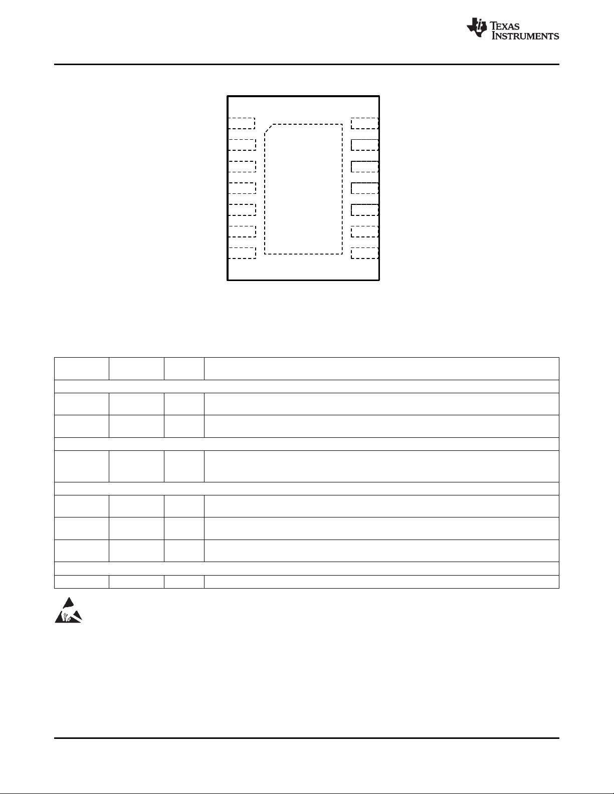
3 mm x 4 mm 14-pin leadless WSON package.
• Small 3 mm x 4 mm 14-pin WSON package
Power is supplied from either a 2.5V or 3.3V supply.
• > 8 kV HBM ESD Rating
• -40 to 85°C operating temperature range
Simplified Application Diagram
1
Please be aware that an important notice concerning availability, standard warranty, and use in critical applications of
Texas Instruments semiconductor products and disclaimers thereto appears at the end of this data sheet.
2All trademarks are the property of their respective owners.
PRODUCTION DATA information is current as of publication date.
Copyright © 2006–2013, Texas Instruments Incorporated
Products conform to specifications per the terms of the Texas
Instruments standard warranty. Production processing does not
necessarily include testing of all parameters.
剩余15页未读,继续阅读


评论0
最新资源