没有合适的资源?快使用搜索试试~ 我知道了~
TI-DS16EV5110A.pdf
需积分: 9 0 下载量 63 浏览量
2022-12-04
00:18:04
上传
评论 4
收藏 3.24MB PDF 举报
温馨提示
试读
25页
TI-DS16EV5110A.pdf
资源详情
资源评论
DS16EV5110A
www.ti.com
SNLS301C –JULY 2008–REVISED APRIL 2013
Video Equalizer (3D+C) for DVI, HDMI Source/Repeater/Sink Applications
Check for Samples: DS16EV5110A
1
FEATURES
DESCRIPTION
The DS16EV5110A is a multi-channel equalizer
2
• 8 Levels of Equalization Settable by 3 Pins or
optimized for video cable extension
Through the SMBus Interface
Source/Repeater/Sink Applications. It operates
• DC-Coupled Inputs and Outputs
between 250Mbps and 2.25Gbps with common
• Optimized for Operation From 250 Mbps to
applications at 1.65Gbps and 2.25Gbps (per data
channel). It contains three Transition-Minimized
2.25 Gbps in Support of UXGA, 480 I/P, 720 I/P,
Differential Signaling (TMDS) data channels and one
1080 I, and 1080 P With 8, 10, and 12-Bit Color
clock channel as specified for DVI and HDMI
Depth Resolutions
interfaces. It provides compensation for skin-effect
• Two DS16EV5110A Devices Support DVI/HDMI
and dielectric losses, a common phenomenon when
Dual Link
transmitting video on commercially available high
• DVI 1.0, and HDMI 1.3a Compatible TMDS
definition video cables.
Interface
The inputs conform to DVI and HDMI requirements
• Clock Channel Signal Detect (LOS)
and features programmable levels of input
equalization. The programmable levels of
• Enable for Power Savings Standby Mode
equalization provide optimal signal boost and reduces
• System Management Bus (SMBus) Provides
inter-symbol interference. Eight levels of boost are
Control of Boost, Output Amplitude, Enable,
selectable via a pin interface or by the optional
and Clock Channel Signal Detect Threshold
System Management Bus.
• Low Power Consumption: 475mW (Typical)
The clock channel is optimized for clock rates of up to
• 0.13 UI Total Jitter at 1.65 Gbps Including
225 MHz and features a signal detect circuit. To
Cable
maximize noise immunity, the DS16EV5110A
features a signal detector with programmable
• Single 3.3V Power Supply
thresholds. The threshold is adjustable through a
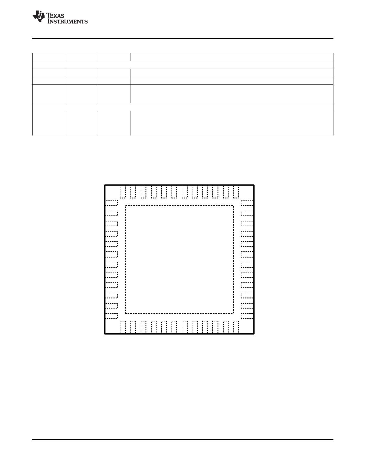
• Small 7mm x 7mm, 48-Pin Leadless WQFN
System Management Bus (SMBus) interface.
Package
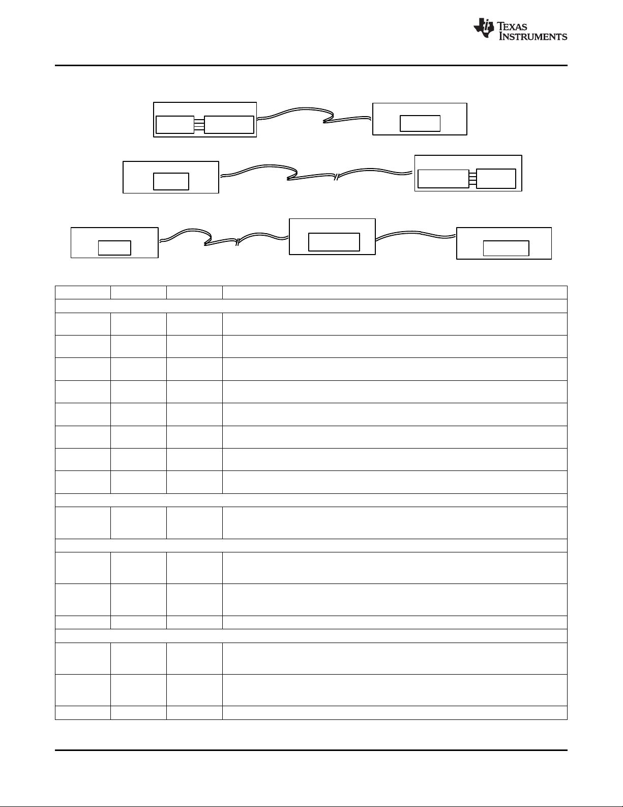
The DS16EV5110A may be used in Source
• -40°C to +85°C Operating Temperature Range
Applications, Sink Applications, or as a Repeater.
• Extends TMDS Cable Reach Over:
The DS16EV5110A also provides support for system
1. > 40 Meters 24 AWG DVI Cable (1.65Gbps)
power management via output enable controls.
2. > 20 Meters 28 AWG DVI Cable (1.65Gbps)
Additional controls are provided via the SMBus
enabling customization and optimization for specific
3. > 20 Meters Cat5/Cat5e/Cat6 Cables
applications requirements. These controls include
(1.65Gbps)
programmable features such as output amplitude and
4. > 20 Meters 28 AWG HDMI Cables
boost controls as well as system level diagnostics.
(2.25Gbps)
The DS16EV5110A is a pin-for-pin replacement to
the DS16EV5110. It features an enhanced CML
APPLICATIONS
output that presents a high impedance when powered
• HDMI / DVI Cable Extenders
down.
• HDMI / DVI Switches
• Projectors
• High Definition Displays
1
Please be aware that an important notice concerning availability, standard warranty, and use in critical applications of
Texas Instruments semiconductor products and disclaimers thereto appears at the end of this data sheet.
2All trademarks are the property of their respective owners.
PRODUCTION DATA information is current as of publication date.
Copyright © 2008–2013, Texas Instruments Incorporated
Products conform to specifications per the terms of the Texas
Instruments standard warranty. Production processing does not
necessarily include testing of all parameters.
DES/Display
Processor
DVI/HDMI Sink
5m 28 AWG DVI/HDMI Cable
DS16EV5110A
DS16EV5110A
DES/Display
Processor
DVI/HDMI Sink
25m 28 AWG DVI/HDMI Cable
SER/A/V
Decoder
DVI/HDMI Source
SER A/V
Decoder
DVI/HDMI Source
SER/A/V
Decoder
DVI/HDMI Source
DES/Display
Processor
DVI/HDMI Sink
25m 28 AWG DVI/HDMI Cable
DS16EV5110A
DVI/HDMI Repeater
1m 28 AWG DVI/HDMI Cable
DS16EV5110A
SNLS301C –JULY 2008–REVISED APRIL 2013
www.ti.com
Typical Application
PIN DESCRIPTIONS
Pin Name Pin Number I/O
(1)
, Type Description
HIGH SPEED DIFFERENTIAL I/O
C_IN− 1 I, CML Inverting and non-inverting TMDS Clock inputs to the equalizer. An on-chip 50Ω terminating
C_IN+ 2 resistor connects C_IN+ to VDD and C_IN- to VDD.
D_IN0− 4 I, CML Inverting and non-inverting TMDS Data inputs to the equalizer. An on-chip 50Ω terminating
D_IN0+ 5 resistor connects D_IN0+ to VDD and D_IN0- to VDD.
D_IN1− 8 I, CML Inverting and non-inverting TMDS Data inputs to the equalizer. An on-chip 50Ω terminating
D_IN1+ 9 resistor connects D_IN1+ to VDD and D_IN1- to VDD.
D_IN2− 11 I, CML Inverting and non-inverting TMDS Data inputs to the equalizer. An on-chip 50Ω terminating
D_IN2+ 12 resistor connects D_IN2+ to VDD and D_IN2- to VDD.
C_OUT- 36 O, CML Inverting and non-inverting TMDS outputs from the equalizer. Open collector.
C_OUT+ 35
D_OUT0− 33 O, CML Inverting and non-inverting TMDS outputs from the equalizer. Open collector.
D_OUT0+ 32
D_OUT1– 29 O, CML Inverting and non-inverting TMDS outputs from the equalizer. Open collector.
D_OUT1+ 28
D_OUT2− 26 O, CML Inverting and non-inverting TMDS outputs from the equalizer. Open collector.
D_OUT2+ 25
Equalization Control
BST_0 23 I, LVCMOS BST_0, BST_1, and BST_2 select the equalizer boost level for EQ channels. BST_0, BST_1,
BST_1 14 and BST_2 are internally pulled Low. See Table 2.
BST_2 37
Device Control
EN 44 I, LVCMOS Enable Equalizer input. When held High, normal operation is selected. When held Low,
standby mode is selected. EN is internally pulled High. Signal is global to all Data and Clock
channels.
FEB 21 I, LVCMOS Force External Boost. When held High, the equalizer boost setting is controlled by the
BST_[0:2] pins. When held Low, the equalizer boost level is controlled through the SMBus
(see Table 1) control pins. FEB is internally pulled High.
SD 45 O, LVCMOS Equalizer Clock Channel Signal Detect Output. Produces a High when signal is detected.
POWER
V
DD
3, 6, 7, Power V
DD
pins should be tied to the V
DD
plane through a low inductance path. A 0.1µF bypass
10, 13, capacitor should be connected between each V
DD
pin to the GND planes.
15, 46
GND 22, 24, GND Ground reference. GND should be tied to a solid ground plane through a low impedance
27, 30, path.
31, 34
Exposed Pad DAP GND The exposed pad at the center of the package must be connected to the ground plane.
(1) Note: I = Input,O = Output, IO =Input/Output,
2 Submit Documentation Feedback Copyright © 2008–2013, Texas Instruments Incorporated
Product Folder Links: DS16EV5110A
DAP = GND
DS16EV5110ASQ
(Top View)
1
2
3
4
5
6
7
8
9
10
11
12
13
14
15
16
17
18
19
20
21
22
23
24
36
35
34
33
32
31
30
29
28
27
26
25
48
47
46
45
44
43
42
41
40
39
38
37
D_IN2+
D_IN2-
D_IN1+
D_IN1-
D_IN0+
D_IN0-
C_IN+
C_IN-
D_OUT2+
D_OUT2-
D_OUT1+
D_OUT1-
D_OUT0+
D_OUT0-
C_OUT+
C_OUT-
VDD
VDD
VDD
VDD GND
GND
GND
GND
VDD
VDD
GND
GND
BST_1
BST_0
CS
SDC
SDA
Reserv
VDD
SD
EN
Reserv
Reserv
Reserv
Reserv
Reserv
Reserv
Reserv
BST_2
Reserv
FEB
Reserv
DS16EV5110A
www.ti.com
SNLS301C –JULY 2008–REVISED APRIL 2013
PIN DESCRIPTIONS (continued)
Pin Name Pin Number I/O
(1)
, Type Description
System Management Bus (SMBus) Interface Control Pins
SDA 18 IO, LVCMOS SMBus Data Input / Output. Internally pulled High to 3.3V with High-Z pull up.
SDC 17 I, LVCMOS SMBus Clock Input. Internally pulled High to 3.3V with High-Z pull up.
CS 16 I, LVCMOS SMBus Chip select. When held High, the equalizer SMBus register is enabled. When held
Low, the equalizer SMBus register is disabled. CS is internally pulled Low. CS is internally
gated with SDC.
Other
Reserv 19, 20, 38, Reserved. Do not connect.
39, 40,41,
42, 43, 47,
48
Connection Diagram
TOP VIEW — Not to Scale
Copyright © 2008–2013, Texas Instruments Incorporated Submit Documentation Feedback 3
Product Folder Links: DS16EV5110A
DS16EV5110A
SNLS301C –JULY 2008–REVISED APRIL 2013
www.ti.com
These devices have limited built-in ESD protection. The leads should be shorted together or the device placed in conductive foam
during storage or handling to prevent electrostatic damage to the MOS gates.
Absolute Maximum Ratings
(1)(2)
Supply Voltage (V
DD
) -0.5V to +4.0V
LVCMOS Input Voltage -0.5V + 4.0V
LVCMOS Output Voltage -0.5V to 4.0V
CML Input/Output Voltage -0.5V to 4.0V
Junction Temperature +150°C
Storage Temperature -65°C to +150°C
Lead Temperature (Soldering, 5 sec.) +260°C
ESD Rating HBM, 1.5 kΩ, 100 pF >6 kV
Thermal Resistance θ
JA
, No Airflow 30°C/W
(1) “Absolute Maximum Ratings” indicate limits beyond which damage to the device may occur, including inoperability and degradation of
device reliability and/or performance. Functional operation of the device and/or non-degradation at the Absolute Maximum Ratings or
other conditions beyond those indicated in the Recommended Operating Conditions is not implied. The Recommended Operating
Conditions indicate conditions at which the device is functional and the device should not be operated beyond such conditions. Absolute
Maximum Numbers are ensured for a junction temperature range of –40°C to +125°C. Models are validated to Maximum Operating
Voltages only.
(2) If Military/Aerospace specified devices are required, please contact the TI Sales Office/Distributors for availability and specifications.
Recommended Operating Conditions
(1) (2)
Min Typ Max Units
Supply Voltage (V
DD
to GND) 3.0 3.3 3.6 V
Ambient Temperature -40 25 +85 °C
(1) Typical values represent most likely parametric norms at V
DD
= 3.3V, T
A
= 25°C, and at the Recommended Operation Conditions at the
time of product characterization and are not ensured.
(2) The Electrical Characteristics tables list ensured specifications under the listed Recommended Operating Conditions except as
otherwise modified or specified by the Electrical Characteristics Conditions and/or Notes.
Electrical Characteristics
Over recommended operating supply and temperature ranges unless other specified.
(1) (2)
Symbol Parameter Conditions Min Typ Max Units
LVCMOS DC SPECIFICATIONS
I
IH-PU
High Level Input Leakage Current LVCMOS pins with internal pull-up
-10 +10 μA
resistors
I
IH-PD
High Level Input Leakage Current LVCMOS pins with internal pull-
80 105 μA
down resistors
I
IL-PU
Low Level Input Leakage Current LVCMOS pins with internal pull-up
-20 -10 μA
resistors
I
IL-PD
Low Level Input Leakage Current LVCMOS pins with internal pull-
-10 +10 μA
down resistors
V
IH
High Level Input Voltage 2.0 VDD V
V
IL
Low Level Input Voltage 0 0.8 V
V
OH
High Level Output Voltage SD Pin, I
OH
= -3mA 2.4 V
V
OL
Low Level Output Voltage SD Pin, I
OL
= 3mA 0.4 V
POWER
PD Power Dissipation EN = High, Device Enabled 475 700 mW
EN = Low, Power Down Mode 70 mW
(1) Typical values represent most likely parametric norms at V
DD
= 3.3V, T
A
= 25°C, and at the Recommended Operation Conditions at the
time of product characterization and are not ensured.
(2) The Electrical Characteristics tables list ensured specifications under the listed Recommended Operating Conditions except as
otherwise modified or specified by the Electrical Characteristics Conditions and/or Notes.
4 Submit Documentation Feedback Copyright © 2008–2013, Texas Instruments Incorporated
Product Folder Links: DS16EV5110A
DS16EV5110A
www.ti.com
SNLS301C –JULY 2008–REVISED APRIL 2013
Electrical Characteristics (continued)
Over recommended operating supply and temperature ranges unless other specified.
(1) (2)
Symbol Parameter Conditions Min Typ Max Units
N Supply Noise Tolerance
(3)
DC to 50MHz 100 mV
P-P
CML INPUTS
V
TX
Input Voltage Swing (Launch Measured differentially at TPA
800 1200 mV
P-P
Amplitude) (Figure 2)
V
ICMDC
Input Common-Mode Voltage DC-Coupled Requirement
V
DD
-0.3 V
DD
-0.2 V
Measured at TPA (Figure 2)
V
IN
Input Voltage Swing Measured differentially at TPB
120 mV
P-P
(Figure 2)
R
LI
Differential Input Return Loss 100 MHz– 825 MHz, with fixture's
10 dB
effect de-embedded
R
IN
Input Resistance IN+ to VDD and IN− to VDD 45 50 55 Ω
CML OUTPUTS
V
O
Output Voltage Swing Measured differentially with OUT+
and OUT− terminated by 50Ω to 800 1200 mV
P-P
VDD
V
OCM
Output common-mode Voltage Measured Single-ended V
DD
-0.3 V
DD
-0.2 V
I
OFF
Output Leakage Current V
OUT
= 3.6V, V
DD
= open or 0V ±1 µA
t
R
, t
F
Transition Time 20% to 80% of differential output
voltage, measured within 1" from 75 240 ps
output pins.
t
CCSK
Inter Pair Channel-to-Channel Difference in 50% crossing
Skew (all 4 Channels) between shortest and longest 25 ps
channels
t
D
Latency 350 ps
OUTPUT JITTER
TJ1 Total Jitter at 1.65 Gbps 20m 28 AWG STP DVI Cable
Data Paths 0.13 0.17 UI
P-P
EQ Setting 0x04 PRBS7
(4) (5) (6)
TJ2 Total Jitter at 2.25 Gbps 20m 28 AWG STP DVI Cable
Data Paths 0.2 UI
P-P
EQ Setting 0x04 PRBS7
(4) (5) (6)
TJ3 Total Jitter at 165 MHz Clock Paths
0.165 UI
P-P
Clock Pattern
(4) (5) (6)
TJ4 Total Jitter at 225 MHz Clock Paths
0.165 UI
P-P
Clock Pattern
(4) (5) (6)
RJ Random Jitter See
(6) (7)
3 ps
rms
BIT RATE
F
CLK
Clock Frequency Clock Path
(4)
25 225 MHz
BR Bit Rate Data Path
(4)
0.25 2.25 Gbps
(3) Allowed supply noise (mV
P-P
sine wave) under typical conditions.
(4) Specification is ensured by characterization and is not tested in production.
(5) Deterministic jitter is measured at the differential outputs (TPC of Figure 2), minus the deterministic jitter before the test channel (TPA of
Figure 2). Random jitter is removed through the use of averaging or similar means.
(6) Total Jitter is defined as peak-to-peak deterministic jitter from
()
+ 14.2 times random jitter in ps
rms
.
(7) Random jitter contributed by the equalizer is defined as sq rt (J
OUT
2
− J
IN
2
). J
OUT
is the random jitter at equalizer outputs in ps
rms
, see
TPC of Figure 2; J
IN
is the random jitter at the input of the equalizer in ps
rms
, see TPA of Figure 2.
Copyright © 2008–2013, Texas Instruments Incorporated Submit Documentation Feedback 5
Product Folder Links: DS16EV5110A
剩余24页未读,继续阅读
安全验证
文档复制为VIP权益,开通VIP直接复制
信息提交成功
评论0
最新资源