没有合适的资源?快使用搜索试试~ 我知道了~
TI-DS64EV400.pdf
需积分: 5 0 下载量 36 浏览量
2022-12-04
00:17:33
上传
评论 3
收藏 3.35MB PDF 举报
温馨提示
试读
22页
TI-DS64EV400.pdf
资源推荐
资源详情
资源评论
ASIC/FPGA
High Speed I/O
Backplane/Cable
Sub-system
Switch Fabric Card
Line Card
OUT
IN
DS64EV400
OUT IN
Tx
Tx
Rx
Rx
ASIC/FPGA
High Speed I/O
DS64EV400
4
4
4
4
DS64EV400
www.ti.com
SNLS281H –AUGUST 2007–REVISED APRIL 2013
DS64EV400 Programmable Quad Equalizer
Check for Samples: DS64EV400
1
FEATURES
DESCRIPTION
The DS64EV400 programmable quad equalizer
2
• Equalizes up to 24 dB Loss at 10 Gbps
provides compensation for transmission medium
• Equalizes up to 22 dB Loss at 6.4 Gbps
losses and reduces the medium-induced deterministic
• 8 Levels of Programmable Equalization
jitter for four NRZ data channels. The DS64EV400 is
optimized for operation up to 10 Gbps for both cables
• Settable through Control Pins or SMBus
and FR4 traces. Each equalizer channel has eight
Tnterface
levels of input equalization that can be programmed
• Operates up to 10 Gbps with 30” FR4 Traces
by three control pins, or individually through a Serial
• Operates up to 6.4 Gbps with 40” FR4 Traces
Management Bus (SMBus) interface.
• 0.175 UI Residual Deterministic Jitter at 6.4
The equalizer supports both AC and DC-coupled data
Gbps with 40” FR4 Traces
paths for long run length data patterns such as
PRBS-31, and balanced codes such as 8b/10b. The
• Single 2.5V or 3.3V Power Supply
device uses differential current-mode logic (CML)
• Signal Detect for Individual Channels
inputs and outputs. The DS64EV400 is available in a
• Standby Mode for Individual Channels
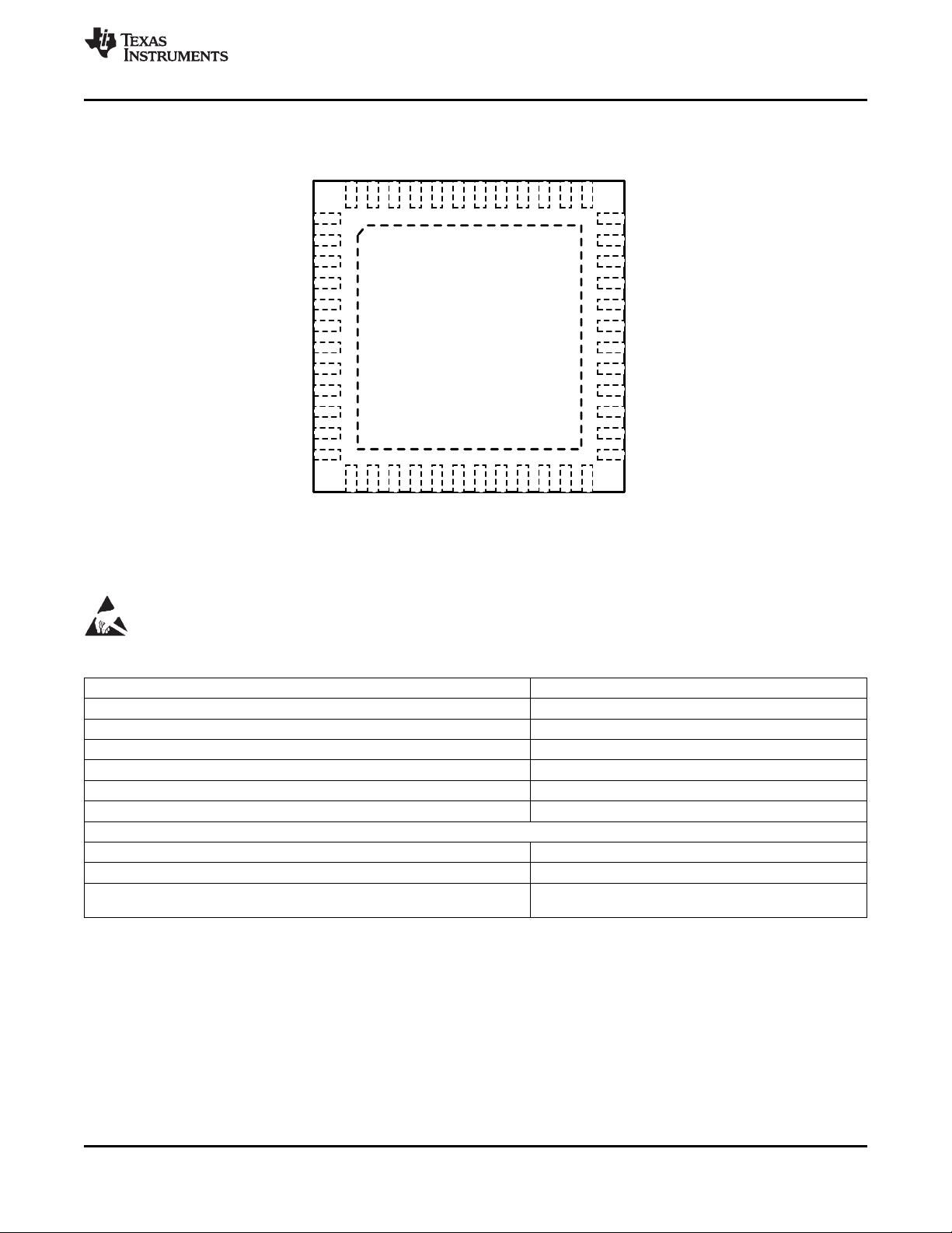
7 mm x 7 mm 48-pin leadless WQFN package.
• Supports AC or DC-Coupling with Wide Input
Power is supplied from either a 2.5V or 3.3V supply.
Common-Mode
• Low Power Consumption: 375 mW Typ at 2.5V
• Small 7 mm x 7 mm 48-Pin WQFN Package
• 9 kV HBM ESD Rating
• -40 to 85°C Operating Temperature Range
Simplified Application Diagram
1
Please be aware that an important notice concerning availability, standard warranty, and use in critical applications of
Texas Instruments semiconductor products and disclaimers thereto appears at the end of this data sheet.
2All trademarks are the property of their respective owners.
PRODUCTION DATA information is current as of publication date.
Copyright © 2007–2013, Texas Instruments Incorporated
Products conform to specifications per the terms of the Texas
Instruments standard warranty. Production processing does not
necessarily include testing of all parameters.
DS64EV400
SNLS281H –AUGUST 2007–REVISED APRIL 2013
www.ti.com
Pin Descriptions
Pin Name Pin No. I/O, Type
(1)
Description
HIGH SPEED DIFFERENTIAL I/O
IN_0+ 1 I, CML Inverting and non-inverting CML differential inputs to the equalizer. An on-chip 100Ω
IN_0– 2 terminating resistor is connected between IN_0+ and IN_0-. Refer to Figure 7.
IN_1+ 4 I, CML Inverting and non-inverting CML differential inputs to the equalizer. An on-chip 100Ω
IN_1– 5 terminating resistor is connected between IN_1+ and IN_1-. Refer to Figure 7.
IN_2+ 8 I, CML Inverting and non-inverting CML differential inputs to the equalizer. An on-chip 100Ω
IN_2– 9 terminating resistor is connected between IN_2+ and IN_2-. Refer to Figure 7.
IN_3+ 11 I, CML Inverting and non-inverting CML differential inputs to the equalizer. An on-chip 100Ω
IN_3– 12 terminating resistor is connected between IN_3+ and IN_3-. Refer to Figure 7.
OUT_0+ 36 O, CML Inverting and non-inverting CML differential outputs from the equalizer. An on-chip 50Ω
OUT_0– 35 terminating resistor connects OUT_0+ to V
DD
and OUT_0- to V
DD
.
OUT_1+ 33 O, CML Inverting and non-inverting CML differential outputs from the equalizer. An on-chip 50Ω
OUT_1– 32 terminating resistor connects OUT_1+ to V
DD
and OUT_1- to V
DD
.
OUT_2+ 29 O, CML Inverting and non-inverting CML differential outputs from the equalizer. An on-chip 50Ω
OUT_2– 28 terminating resistor connects OUT_2+ to V
DD
and OUT_2- to V
DD
.
OUT_3+ 26 O, CML Inverting and non-inverting CML differential outputs from the equalizer. An on-chip 50Ω
OUT_3– 25 terminating resistor connects OUT_3+ to V
DD
and OUT_3- to V
DD
.
EQUALIZATION CONTROL
BST_2 37 I, LVCMOS BST_2, BST_1, and BST_0 select the equalizer strength for all EQ channels. BST_2 is
BST_1 14 internally pulled high. BST_1 and BST_0 are internally pulled low.
BST_0 23
DEVICE CONTROL
EN0 44 I, LVCMOS Enable Equalizer Channel 0 input. When held High, normal operation is selected. When held
Low, standby mode is selected. EN is internally pulled High.
EN1 42 I, LVCMOS Enable Equalizer Channel 1 input. When held High, normal operation is selected. When held
Low, standby mode is selected. EN is internally pulled High.
EN2 40 I, LVCMOS Enable Equalizer Channel 2 input. When held High, normal operation is selected. When held
Low, standby mode is selected. EN is internally pulled High.
EN3 38 I, LVCMOS Enable Equalizer Channel 3 input. When held High, normal operation is selected. When held
Low, standby mode is selected. EN is internally pulled High.
FEB 21 I, LVCMOS Force External Boost. When held high, the equalizer boost setting is controlled by BST_[2:0]
pins. When held low, the equalizer boost setting is controlled by SMBus (Table 1) register bits.
FEB is internally pulled High.
SD0 45 O, LVCMOS Equalizer Ch0 Signal Detect Output. Produces a High when signal is detected.
SD1 43 O, LVCMOS Equalizer Ch1 Signal Detect Output. Produces a High when signal is detected.
SD2 41 O, LVCMOS Equalizer Ch2 Signal Detect Output. Produces a High when signal is detected.
SD3 39 O, LVCMOS Equalizer Ch3 Signal Detect Output. Produces a High when signal is detected.
POWER
V
DD
3, 6, 7, Power V
DD
= 2.5V ± 5% or 3.3V ± 10%. V
DD
pins should be tied to V
DD
plane through low inductance
10, 13, path. A 0.01μF bypass capacitor should be connected between each V
DD
pin to GND planes.
15, 46
GND 22, 24, Power Ground reference. GND should be tied to a solid ground plane through a low impedance path.
27, 30,
31, 34
DAP PAD Power Ground reference. The exposed pad at the center of the package must be connected to ground
plane of the board.
SERIAL MANAGEMENT BUS (SMBus) INTERFACE CONTROL PINS
SDA 18 I/O, LVCMOS Data input/output (bi-directional). Internally pulled high.
SDC 17 I, LVCMOS Clock input. Internally pulled high.
CS 16 I, LVCMOS Chip select. When pulled high, access to the equalizer SMBus registers are enabled. When
pulled low, access to the equalizer SMBus registers are disabled. Please refer to “ SMBus
configuration Registers” section for detail information.
Other
Reserv 19, 20 Reserved. Do not connect.
47,48
(1) Note: I = Input O = Output
2 Submit Documentation Feedback Copyright © 2007–2013, Texas Instruments Incorporated
Product Folder Links: DS64EV400
1
2
3
4
5
6
7
8
9
10
11
12
13
14
15
16
17
18
19
20
21
22
23
24
36
35
34
33
32
31
30
29
28
27
26
25
48
47
46
45
44
43
42
41
40
39
38
37
IN_3-
IN_3+
IN_2-
IN_2+
IN_1-
IN_1+
IN_0-
IN_0+
OUT_3-
OUT_3+
OUT_2-
OUT_2+
OUT_1-
OUT_1+
OUT_0-
OUT_0+
V
DD
V
DD
V
DD
V
DD
GND
GND
GND
GND
V
DD
V
DD
GND
GND
BST_1
BST_0
CS
SDC
SDA
Reserv
V
DD
SD0
EN0
SD1
EN1
SD2
EN2
SD3
EN3
Reserv
BST_2
Reserv
Reserv
FEB
DS64EV400
TOP VIEW
DAP = GND
DS64EV400
www.ti.com
SNLS281H –AUGUST 2007–REVISED APRIL 2013
Connection Diagram
Figure 1. WQFN Package
See Package Number NJU0048D
These devices have limited built-in ESD protection. The leads should be shorted together or the device placed in conductive foam
during storage or handling to prevent electrostatic damage to the MOS gates.
Absolute Maximum Ratings
(1)(2)
Supply Voltage (V
DD
) −0.5V to +4.0V
CMOS Input Voltage −0.5V + 4.0V
CMOS Output Voltage −0.5V to 4.0V
CML Input/Output Voltage −0.5V to 4.0V
Junction Temperature +150°C
Storage Temperature −65°C to +150°C
Lead Temperature (Soldering, 4 Seconds) +260°C
ESD Rating
HBM, 1.5 kΩ, 100 pF > 9 kV
EIAJ, 0Ω, 200 pF > 250V
Thermal Resistance
θ
JA
, No Airflow 30°C/W
(1) “Absolute Maximum Ratings” indicate limits beyond which damage to the device may occur, including inoperability and degradation of
device reliability and/or performance. Functional operation of the device and/or non-degradation at the Absolute Maximum Ratings or
other conditions beyond those indicated in the Recommended Operating Conditions is not implied. The Recommended Operating
Conditions indicate conditions at which the device is functional and the device should not be operated beyond such conditions. Absolute
Maximum Numbers are ensured for a junction temperature range of -40°C to +125°C. Models are validated to Maximum Operating
Voltages only.
(2) If Military/Aerospace specified devices are required, please contact the Texas Instruments Sales Office/ Distributors for availability and
specifications.
Copyright © 2007–2013, Texas Instruments Incorporated Submit Documentation Feedback 3
Product Folder Links: DS64EV400
DS64EV400
SNLS281H –AUGUST 2007–REVISED APRIL 2013
www.ti.com
Recommended Operating Conditions
Min Typ Max Units
Supply Voltage V
DD2.5
to GND 2.375 2.5 2.625 V
V
DD3.3
to GND 3.0 3.3 3.6 V
Ambient Temperature −40 25 +85 °C
Electrical Characteristics
Over recommended operating supply and temperature ranges with default register settings unless other specified.
Parameter Test Conditions Min Typ
(1)
Max Units
POWER
P Power Supply Consumption Device Output Enabled
490 700 mW
(EN [0–3] = High), V
DD3.3
(2)
Device Output Disable
100 mW
(EN [0–3] = Low), V
DD3.3
P Power Supply Consumption Device Output Enabled
360 490 mW
(EN [0–3] = High), V
DD2.5
(2)
Device Output Disable
30
(EN [0–3] = Low), V
DD2.5
(2)
N Supply Noise Tolerance
(3)
50 Hz — 100 Hz 100 mV
P-P
100 Hz — 10 MHz 40 mV
P-P
10 MHz — 1.6 GHz 10 mV
P-P
LVCMOS DC SPECIFICATIONS
V
IH
High Level Input Voltage V
DD3.3
2.0 V
DD3.3
V
V
DD2.5
1.6 V
DD2.5
V
V
IL
Low Level Input Voltage -0.3 0.8 V
V
OH
High Level Output Voltage I
OH
= -3mA, V
DD3.3
2.4 V
I
OH
= -3mA, V
DD2.5
2.0
V
OL
Low Level Output Voltage I
OL
= 3mA 0.4 V
I
IN
Input Leakage Current V
IN
= V
DD
+15 μA
V
IN
= GND -15 μA
I
IN-P
Input Leakage Current with Internal V
IN
= V
DD
, with internal pull-down resistors +120 μA
Pull-Down/Up Resistors
V
IN
= GND, with internal pull-up resistors -20 μA
SIGNAL DETECT
SDH Signal Detect ON Threshold Level Default input signal level to assert SD pin, 6.4 70 mV
p-p
Gbps
SDI Signal Detect OFF Threshold Level Default input signal level to de-assert SD, 6.4 40 mV
p-p
Gbps
CML RECEIVER INPUTS (IN_n+, IN_n-)
V
TX
Source Transmit Launch Signal Level AC-Coupled or DC-Coupled Requirement,
(IN diff) Differential measurement at point A. 400 1600 mV
P-P
Figure 2
V
INTRE
Input Threshold Voltage Differential measurement at
120 mV
P-P
point B. Figure 2
V
DDTX
Supply Voltage of Transmitter to EQ DC-Coupled Requirement
(4)
1.6 V
DD
V
V
ICMDC
Input Common Mode Voltage DC-Coupled Requirement, Differential V
DDTX
– V
DDTX
V
measurement at point A. Figure 2,
(5)
0.8 – 0.2
R
LI
Differential Input Return Loss 100 MHz – 3.2 GHz, with fixture’s effect de-
10 dB
embedded
(1) Typical values represent most likely parametric norms at V
DD
= 3.3V or 2.5V, T
A
= 25°C, and at the Recommended Operation
Conditions at the time of product characterization and are not ensured.
(2) The V
DD2.5
is V
DD
= 2.5V ± 5% and V
DD3.3
is V
DD
= 3.3V ± 10%.
(3) Allowed supply noise (mV
P-P
sine wave) under typical conditions.
(4) Recommended value. Parameter not tested in production.
(5) Measured with clock-like {11111 00000} pattern.
4 Submit Documentation Feedback Copyright © 2007–2013, Texas Instruments Incorporated
Product Folder Links: DS64EV400
DS64EV400
www.ti.com
SNLS281H –AUGUST 2007–REVISED APRIL 2013
Electrical Characteristics (continued)
Over recommended operating supply and temperature ranges with default register settings unless other specified.
Parameter Test Conditions Min Typ
(1)
Max Units
R
IN
Input Resistance Differential across IN+ and IN-, Figure 7 85 100 115 Ω
CML OUTPUTS (OUT_n+, OUT_n-)
V
OD
Output Differential Voltage Level Differential measurement with OUT+ and OUT-
(OUT diff) terminated by 50Ω to GND, AC-Coupled 500 620 725 mV
P-P
Figure 3
V
OCM
Output Common Mode Voltage Single-ended measurement DC-Coupled with V
DD
– V
DD
–
V
50Ω terminations
(5)
0.2 0.1
t
R
, t
F
Transition Time 20% to 80% of differential output voltage,
measured within 1” from output pins. 20 60 ps
Figure 3,
(5)
R
O
Output Resistance Single ended to V
DD
42 50 58 Ω
R
LO
Differential Output Return Loss 100 MHz – 1.6 GHz, with fixture’s effect de-
10 dB
embedded. IN+ = static high.
t
PLHD
Differential Low to High Propagation Propagation delay measurement at 50% VO
240 ps
Delay between input to output, 100 Mbps. Figure 4,
(5)
t
PHLD
Differential High to Low Propagation
240 ps
Delay
t
CCSK
Inter Pair Channel to Channel Skew Difference in 50% crossing between channels 7 ps
t
PPSK
Part to Part Output Skew Difference in 50% crossing between outputs 20 ps
EQUALIZATION
DJ1 Residual Deterministic Jitter 30” of 6 mil microstrip FR4,
0.20 UI
P-P
at 10 Gbps EQ Setting 0x06, PRBS-7 (2
7
-1) pattern.
(6)
DJ2 Residual Deterministic Jitter 40” of 6 mil microstrip FR4,
0.17 0.26 UI
P-P
at 6.4 Gbps EQ Setting 0x06, PRBS-7 (2
7
-1) pattern.
(7)(6)
DJ3 Residual Deterministic Jitter 40” of 6 mil microstrip FR4,
0.12 0.20 UI
P-P
at 5 Gbps EQ Setting 0x07, PRBS-7 (2
7
-1) pattern.
(7) (6)
DJ4 Residual Deterministic Jitter 40” of 6 mil microstrip FR4,
0.1 0.16 UI
P-P
at 2.5 Gbps EQ Setting 0x07, PRBS-7 (2
7
-1) pattern.
(7)(6)
RJ Random Jitter See
(8)(9)
0.5 psrms
SIGNAL DETECT and ENABLE TIMING
t
ZISD
Input OFF to ON detect — SD Output Response time measurement at V
IN
to SD
35 ns
High Response Time output, V
IN
= 800 mV
P-P
, 100 Mbps, 40” of 6 mil
microstrip FR4
t
IZSD
Input ON to OFF detect — SD Output
400 ns
Figure 2 and Figure 5,
(8)
Low Response Time
t
OZOED
EN High to Output ON Response Response time measurement at EN input to
150 ns
Time V
O
, V
IN
= 800 mV
P-P
, 100 Mbps, 40” of 6 mil
microstrip FR4
t
ZOED
EN Low to Output OFF Response
5 ns
Figure 2 and Figure 7,
(8)
Time
(6) Deterministic jitter is measured at the differential outputs (point C of Figure 2), minus the deterministic jitter before the test channel (point
A of Figure 2). Random jitter is removed through the use of averaging or similar means.
(7) Specification is ensured by characterization at optimal boost setting and is not tested in production.
(8) Measured with clock-like {11111 00000} pattern.
(9) Random jitter contributed by the equalizer is defined as sqrt (J
OUT
2
– J
IN
2
). J
OUT
is the random jitter at equalizer outputs in ps-rms, see
point C of Figure 2; J
IN
is the random jitter at the input of the equalizer in ps-rms, see point B of Figure 2.
Copyright © 2007–2013, Texas Instruments Incorporated Submit Documentation Feedback 5
Product Folder Links: DS64EV400
剩余21页未读,继续阅读
资源评论
不觉明了
- 粉丝: 3236
- 资源: 5614
上传资源 快速赚钱
- 我的内容管理 展开
- 我的资源 快来上传第一个资源
- 我的收益 登录查看自己的收益
- 我的积分 登录查看自己的积分
- 我的C币 登录后查看C币余额
- 我的收藏
- 我的下载
- 下载帮助
最新资源
- java-leetcode题解之第111题二叉树的最小深度.zip
- java-leetcode题解之第110题平衡二叉树.zip
- java-leetcode题解之第109题有序链表转换二叉搜索树.zip
- java-leetcode题解之第108题将有序数组转换为二叉搜索树.zip
- java-leetcode题解之第107题二叉树的层序遍历II.zip
- java-leetcode题解之第102题二叉树的层序遍历.zip
- java-leetcode题解之第103题二叉树的锯齿形层序遍历.zip
- java-leetcode题解之第104题二叉树的最大深度.zip
- java-leetcode题解之第173题二叉搜索树迭代器.zip
- java-leetcode题解之第100题相同的树.zip
资源上传下载、课程学习等过程中有任何疑问或建议,欢迎提出宝贵意见哦~我们会及时处理!
点击此处反馈
安全验证
文档复制为VIP权益,开通VIP直接复制
信息提交成功