TI-DS90CP04.pdf
需积分: 5 155 浏览量
2022-12-03
09:47:04
上传
评论 4
收藏 948KB PDF 举报

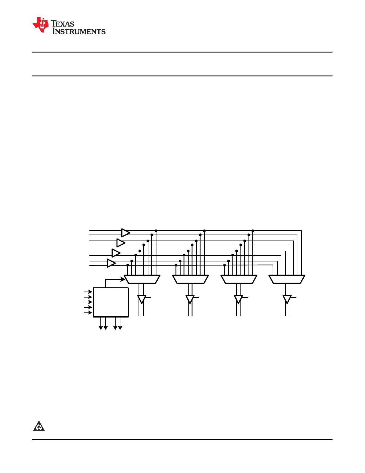
IN1+
IN1-
IN2+
IN2-
IN3+
IN3-
IN4+
IN4-
OUT1+
OUT1-
OUT2+
OUT2-
OUT3+
OUT3-
OUT4+
OUT4-
SCLK
SI/SEL1
CSO
CSCLK
EN1 EN2 EN3 EN4
4:1 MUX1
4:1 MUX2 4:1 MUX3
4:1 MUX4
LOAD
MODE
Digital Control
Interface
RSO
RSCLK
SEL0
DS90CP04
www.ti.com
SNLS154I –JANUARY 2002–REVISED APRIL 2013
DS90CP04 1.5 Gbps 4x4 LVDS Crosspoint Switch
Check for Samples: DS90CP04
1
FEATURES
DESCRIPTION
DS90CP04 is a 4x4 digital cross-point switch with
2
• DC - 1.5 Gbps Low Jitter, Low Skew Operation
broadside input and output pins for efficient board
• Pin and Serial Interface Configurable, Fully
layout. It utilizes Low Voltage Differential Swing
Differential, Non-blocking Architecture
(LVDS) technology for low power, high-speed
• Wide Input Common Mode Voltage Range
operation. Data paths are fully differential from input
to output for low noise. The non-blocking architecture
Enables Easy Interface to LVDS/LVPECL/2.5V-
allows connections of any input to any output or
CML Drivers
outputs. The switch matrix consists of four differential
• TRI-STATE LVDS Outputs
4:1 multiplexes. Each output channel connects to one
• Serial Control Interface with Read-back
of the four inputs common to all multiplexers.
Capability
A simple serial control interface or a configuration
• Double Register Loading
select port is activated by the state of the MODE pin.
• Single +2.5V Supply
When utilizing the serial control interface a single
load command will update the new switch
• Small 6x6 mm WQFN-32 Space Saving
configuration for all outputs simultaneously.
Package
• Fabricated with Advanced CMOS Process
Technology
Functional Block Diagrams
1
Please be aware that an important notice concerning availability, standard warranty, and use in critical applications of
Texas Instruments semiconductor products and disclaimers thereto appears at the end of this data sheet.
2All trademarks are the property of their respective owners.
PRODUCTION DATA information is current as of publication date.
Copyright © 2002–2013, Texas Instruments Incorporated
Products conform to specifications per the terms of the Texas
Instruments standard warranty. Production processing does not
necessarily include testing of all parameters.

剩余23页未读,继续阅读
资源评论


