没有合适的资源?快使用搜索试试~ 我知道了~
TI-SN55LVCP22.pdf
需积分: 5 0 下载量 163 浏览量
2022-12-03
09:44:10
上传
评论 4
收藏 1.29MB PDF 举报
温馨提示
试读
25页
TI-SN55LVCP22.pdf
资源推荐
资源详情
资源评论
SN55LVCP22 QML Class Q 2×2 1-Gbps LVDS Crosspoint Switch
1 Features
• QML class Q, SMD 5962-11242
• High-speed (up to 1000 Mbps)
• Low-jitter fully differential data path
• 50 ps (typ), of peak-to-peak jitter with
PRBS = 2
23
–1 pattern
• Less than 227 mW (typ), 313 mW (max) total
power dissipation
• Output (channel-to-channel) skew is 80 ps (typ)
• Configurable as 2:1 mux, 1:2 demux, repeater or
1:2 signal splitter
• Inputs accept LVDS, LVPECL, and CML signals
• Fast switch time of 1.7 ns (typ)
• Fast propagation delay of 0.65 ns (typ)
• Inter-operates with TIA/EIA-644-A LVDS standard
• Supports defense, aerospace, and medical
applications:
– Controlled baseline
– One assembly/test site and one fabrication site
– Extended product life cycle and extended
product-change notification
– Product traceability
2 Applications
• Global positioning system receiver
• Defense radio
• Sonar
• Seeker front end
• Radar
3 Description
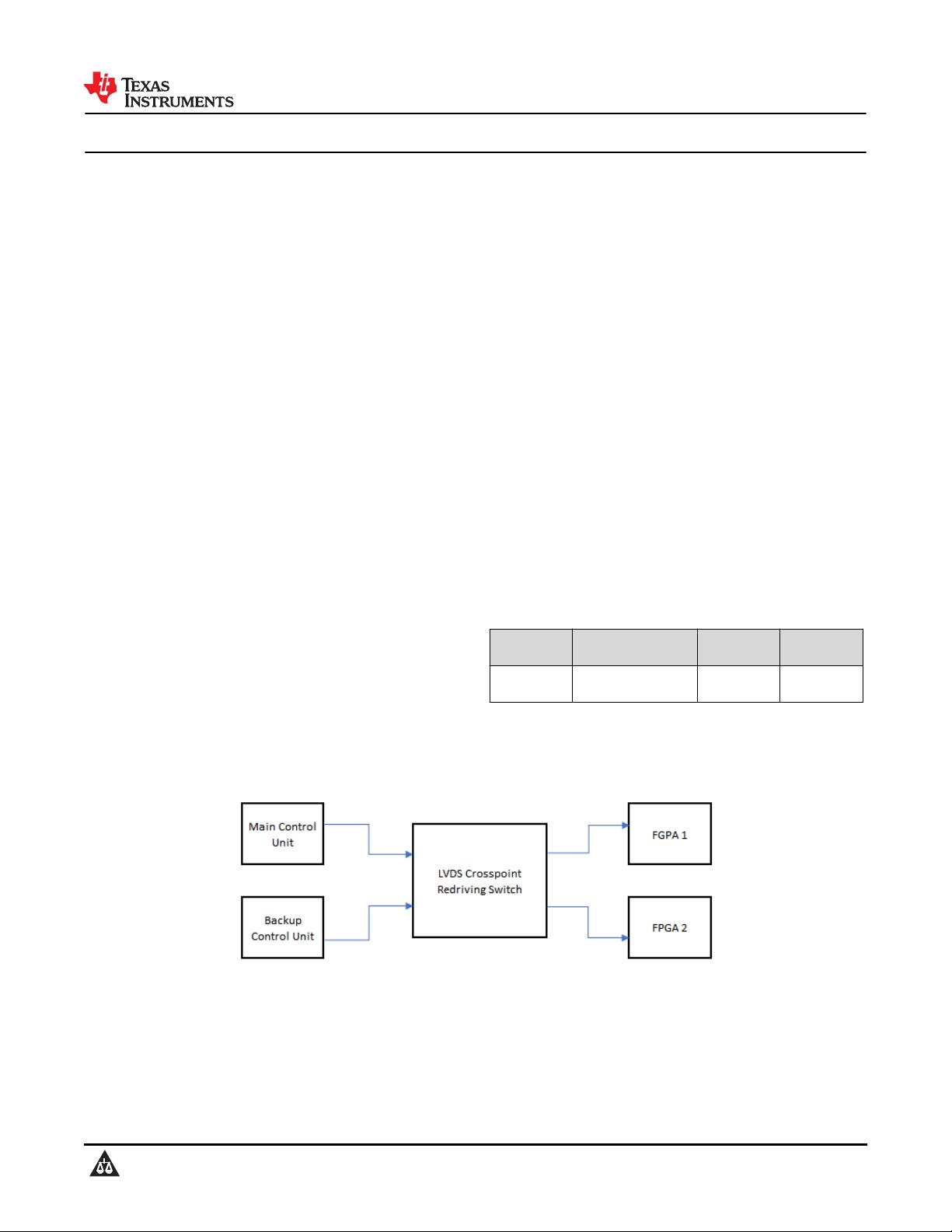
The SN55LVCP22 is a 2×2 crosspoint switch
providing greater than 1000 Mbps operation for each
path. The dual channels incorporate wide common-
mode (0 V to 4 V) receivers, allowing for the receipt of
LVDS, LVPECL, and CML signals. The dual outputs
are LVDS drivers to provide low-power, low-EMI, high-
speed operation. The SN55LVCP22 provides a single
device supporting 2:2 buffering (repeating), 1:2
splitting, 2:1 multiplexing, 2×2 switching, and
LVPECL/CML to LVDS level translation on each
channel. The flexible operation of the SN55LVCP22
provides a single device to support the redundant
serial bus transmission needs (working and protection
switching cards) of fault-tolerant switch systems found
in optical networking, wireless infrastructure, and data
communications systems.
The SN55LVCP22 uses a fully differential data path to
ensure low-noise generation, fast switching times, low
pulse width distortion, and low jitter. Output channel-
to- channel skew is 80 ps (typ) to ensure accurate
alignment of outputs in all applications.
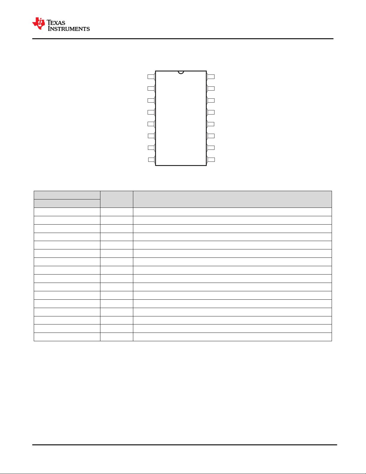
Device Information
PART
NUMBER
GRADE PACKAGE
(1)
BODY SIZE
(NOM)
5962-112420
1QFA
QMLQ CFP (16)
6.73 mm x
10.3 mm
(1) For all available packages, see the orderable addendum at
the end of the data sheet.
Simplified Application
www.ti.com
SN55LVCP22
SLLSFJ2 – SEPTEMBER 2020
Copyright © 2020 Texas Instruments Incorporated
Submit Document Feedback
1
Product Folder Links: SN55LVCP22
SN55LVCP22
SLLSFJ2 – SEPTEMBER 2020
An IMPORTANT NOTICE at the end of this data sheet addresses availability, warranty, changes, use in safety-critical applications,
intellectual property matters and other important disclaimers. PRODUCTION DATA.
Table of Contents
1 Features............................................................................1
2 Applications..................................................................... 1
3 Description.......................................................................1
4 Revision History.............................................................. 2
5 Pin Configuration and Functions...................................3
6 Specifications.................................................................. 4
6.1 Absolute Maximum Ratings........................................ 4
6.2 Handling Ratings.........................................................4
6.3 Recommended Operating Conditions.........................4
6.4 Thermal Information....................................................4
6.5 Electrical Characteristics ............................................4
6.6 Switching Characteristics............................................6
6.7 Typical Characteristics................................................ 7
7 Parameter Measurement Information.......................... 10
8 Detailed Description......................................................14
8.1 Overview................................................................... 14
8.2 Functional Block Diagram......................................... 14
8.3 Feature Description...................................................14
8.4 Device Functional Modes..........................................14
9 Application and Implementation.................................. 16
9.1 Application Information............................................. 16
9.2 Typical Application.................................................... 16
10 Power Supply Recommendations..............................19
11 Layout........................................................................... 20
11.1 Layout Guidelines................................................... 20
11.2 Layout Example...................................................... 20
12 Device and Documentation Support..........................21
12.1 Trademarks.............................................................21
12.2 Electrostatic Discharge Caution..............................21
12.3 Glossary..................................................................21
13 Mechanical, Packaging, and Orderable
Information.................................................................... 21
4 Revision History
NOTE: Page numbers for previous revisions may differ from page numbers in the current version.
DATE REVISION NOTES
September 2020 * Initial Release
SN55LVCP22
SLLSFJ2 – SEPTEMBER 2020
www.ti.com
2 Submit Document Feedback
Copyright © 2020 Texas Instruments Incorporated
Product Folder Links: SN55LVCP22
5 Pin Configuration and Functions
1
2
3
4
5
6
7
8
9
10
11
12
13
14
15
16
SEL1
SEL0
IN0+
IN0-
VCC
IN1+
IN1-
NC NC
OUT1-
OUT1+
GND
OUT0-
OUT0+
EN1
EN0
NC - No internal connection
W PACKAGE
(TOP VIEW)
Pin Functions
TERMINAL
I/O DESCRIPTION
NAME NO.
SEL1 1 Input Switch Selection Control 1
SEL0 2 Input Switch Selection Control 2
IN0+ 3 Input LVDS Receiver Positive Input 0
IN0- 4 Input LVDS Receiver Negative Input 0
VCC 5 Power 3.3V Supply Voltage
IN1+ 6 Input LVDS Receiver Positive Input 1
IN1- 7 Input LVDS Receiver Negative Input 1
NC 8 N/A No Internal Connection
NC 9 N/A No Internal Connection
OUT1- 10 Output LVDS Driver Negative Output 1
OUT1+ 11 Output LVDS Driver Positive Output 1
GND 12 Ground Ground
OUT0- 13 Output LVDS Driver Negative Output 0
OUT0+ 14 Output LVDS Driver Positive Output 0
EN1 15 Input Output Enable for Driver 1
EN0 16 Input Output Enable for Driver 0
www.ti.com
SN55LVCP22
SLLSFJ2 – SEPTEMBER 2020
Copyright © 2020 Texas Instruments Incorporated
Submit Document Feedback
3
Product Folder Links: SN55LVCP22
6 Specifications
6.1 Absolute Maximum Ratings
over operating free-air temperature range unless otherwise noted
(1)
UNIT
Supply voltage
(2)
, V
CC
–0.5 V to 4 V
CMOS/TTL input voltage (ENO, EN1, SEL0, SEL1) –0.5 V to 4 V
LVDS receiver input voltage (IN+, IN–) –0.7 V to 4.3 V
LVDS driver output voltage (OUT+, OUT–) –0.5 V to 4 V
LVDS output short circuit current Continuous
Maximum Junction temperature 150°C
(1) Stresses beyond those listed under absolute maximum ratings may cause permanent damage to the device. These are stress ratings
only, and functional operation of the device at these or any other conditions beyond those indicated under recommended operating
conditions is not implied. Exposure to absolute-maximum-rated conditions for extended periods may affect device reliability.
(2) All voltage values, except differential I/O bus voltages, are with respect to network ground terminals.
6.2 Handling Ratings
MIN MAX UNIT
T
stg
Storage temperature range -65 125 °C
V
(ESD)
Electrostatic discharge
Human body model (HBM), per ANSI/ESDA/JEDEC JS-001, all
pins
(1)
-5000 5000
V
Charged device model (CDM), per JEDEC specification
JESD22-C101, all pins
(2)
-500 500
(1) JEDEC document JEP155 states that 500-V HBM allows safe manufacturing with a standard ESD control process.
(2) JEDEC document JEP157 states that 250-V CDM allows safe manufacturing with a standard ESD control process.
6.3 Recommended Operating Conditions
MIN
NOM MAX UNIT
Supply voltage, V
CC
3 3.3 3.6 V
Receiver input voltage 0 4 V
Operating case (top) temperature, T
C
(1)
–55 125 °C
Magnitude of differential input voltage, |V
ID
| 0.1 3 V
(1) Maximum case temperature operation is allowed as long as the device maximum junction temperature is not exceeded.
6.4 Thermal Information
THERMAL METRIC
(1)
SN55LVCP22A-SP
UNITW (CFP)
16 PINS
R
θJA
Junction-to-ambient thermal resistance 118.1 °C/W
R
θJC(top)
Junction-to-case (top) thermal resistance 51.2 °C/W
R
θJB
Junction-to-board thermal resistance 107.2 °C/W
ψ
JT
Junction-to-top characterization parameter 28.4 °C/W
ψ
JB
Junction-to-board characterization parameter 95.1 °C/W
(1) For more information about traditional and new thermal metrics, see the Semiconductor and IC Package Thermal Metrics application
report.
6.5 Electrical Characteristics
over recommended operating conditions unless otherwise noted
PARAMETER TEST CONDITIONS MIN TYP
(1)
MAX UNIT
CMOS/TTL DC SPECIFICATIONS (EN0, EN1, SEL0, SEL1)
V
IH
High-level input voltage 2 1.5 V
CC
V
SN55LVCP22
SLLSFJ2 – SEPTEMBER 2020
www.ti.com
4 Submit Document Feedback
Copyright © 2020 Texas Instruments Incorporated
Product Folder Links: SN55LVCP22
over recommended operating conditions unless otherwise noted
PARAMETER TEST CONDITIONS MIN TYP
(1)
MAX UNIT
V
IL
Low-level input voltage GND 1.5 0.8 V
I
IH
High-level input current V
IN
= 3.6 V or 2.0 V, V
CC
= 3.6 V -25 ±3 25 µA
I
IL
Low-level input current V
IN
= 0.0 V or 0.8 V, V
CC
= 3.6 V -15 ±1 15 µA
V
CL
Input clamp voltage I
CL
= –18 mA -0.8 -1.5 V
LVDS OUTPUT SPECIFICATIONS (OUT0, OUT1)
|V
OD
| Differential output voltage
R
L
= 75 Ω, See Figure 7-3 255 390 475
mV
R
L
= 75 Ω, V
CC
= 3.3 V, T
A
= 25°C, See
Figure 7-3
320 390 430
Δ|V
OD
|
Change in differential output voltage magnitude
between logic states
V
ID
= ±100 mV, See Figure 7-3 –25 25 mV
V
OS
Steady-state offset voltage See Figure 7-4 1 1.2 1.45 V
ΔV
OS
Change in steady-state offset voltage between
logic states
See Figure 7-4 –25 25 mV
V
OC(PP)
Peak-to-peak common-mode output voltage See Figure 7-4 50 mV
I
OZ
High-impedance output current V
OUT
= GND or V
CC
-15 15 µA
I
OFF
Power-off leakage current V
CC
= 0 V, 1.5 V; V
OUT
= 3.6 V or GND -15 15 µA
I
OS
Output short-circuit current V
OUT+
or V
OUT-
= 0 V -8 mA
I
OSB
Both outputs short-circuit current V
OUT+
and V
OUT-
= 0 V –8 8 mA
C
O
Differential output capacitance V
I
= 0.4 sin(4E6πt) + 0.5 V 3 pF
LVDS RECEIVER DC SPECIFICATIONS (IN0, IN1)
V
TH
Positive-going differential input voltage threshold See Figure 7-2 and Table 7-1 100 mV
V
TL
Negative-going differential input voltage threshold See Figure 7-2 and Table 7-1 –100 mV
V
ID(HYS)
Differential input voltage hysteresis 20 150 mV
V
CMR
Common-mode voltage range V
ID
= 100 mV, V
CC
= 3.0 V to 3.6 V 0.05 3.95 V
I
IN
Input current
V
IN
= 4 V, V
CC
= 3.6 V or 0.0 -18 ±1 18
µA
V
IN
= 0 V, V
CC
= 3.6V or 0.0 -18 ±1 18
C
IN
Differential input capacitance V
I
= 0.4 sin (4E6πt) + 0.5 V 3 pF
SUPPLY CURRENT
I
CCQ
Quiescent supply current R
L
= 75 Ω, EN0=EN1=High 60 87 mA
I
CCD
Total supply current
R
L
= 75 Ω, C
L
= 5 pF, 500 MHz (1000
Mbps), EN0=EN1=High
63 87 mA
I
CCZ
3-state supply current EN0 = EN1 = Low 25 35 mA
(1) All typical values are at 25°C and with a 3.3-V supply.
www.ti.com
SN55LVCP22
SLLSFJ2 – SEPTEMBER 2020
Copyright © 2020 Texas Instruments Incorporated
Submit Document Feedback
5
Product Folder Links: SN55LVCP22
剩余24页未读,继续阅读
资源评论
不觉明了
- 粉丝: 3235
- 资源: 5614
上传资源 快速赚钱
- 我的内容管理 展开
- 我的资源 快来上传第一个资源
- 我的收益 登录查看自己的收益
- 我的积分 登录查看自己的积分
- 我的C币 登录后查看C币余额
- 我的收藏
- 我的下载
- 下载帮助
安全验证
文档复制为VIP权益,开通VIP直接复制
信息提交成功